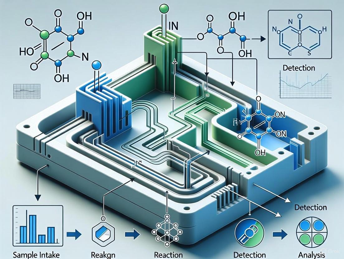
3D Printed Microfluidic Chips with Smartphone Detection: A Revolutionary Approach for Environmental Drug Monitoring
This article explores the convergence of 3D printing, microfluidics, and smartphone-based detection to create portable, cost-effective analytical systems for monitoring pharmaceutical residues in the environment.
3D Printed Microfluidic Chips with Smartphone Detection: A Revolutionary Approach for Environmental Drug Monitoring
Abstract
This article explores the convergence of 3D printing, microfluidics, and smartphone-based detection to create portable, cost-effective analytical systems for monitoring pharmaceutical residues in the environment. Aimed at researchers, scientists, and drug development professionals, it provides a comprehensive overview from foundational principles to advanced applications. We detail the design and fabrication of 3D-printed microfluidic chips, the integration of smartphone colorimetry and spectrophotometry for on-site analysis, and the optimization of these systems for detecting drugs like Baclofen and Doxorubicin in complex matrices. The content further addresses troubleshooting common fabrication and detection challenges, validates the performance of these integrated systems against traditional methods, and discusses the transformative potential of this technology for enabling real-time, accessible environmental surveillance.
The Convergence of 3D Printing, Microfluidics, and Smartphone Sensing
Core Physical Principles
The operation of microfluidic devices, especially within the context of 3D-printed chips for environmental drug research, is governed by unique physical phenomena that dominate at the microscale. Understanding these principles is fundamental to designing effective and reliable lab-on-a-chip systems.
Laminar Flow and the Reynolds Number
In microfluidic channels, fluid flow is characterized as laminar, meaning fluids move in smooth, parallel layers without chaotic mixing [1]. This behavior is quantitatively described by the Reynolds number (Re), a dimensionless quantity representing the ratio of inertial forces to viscous forces [1] [2]. The table below summarizes key aspects of laminar flow in microfluidics.
Table 1: Characteristics of Laminar Flow in Microfluidics
| Parameter | Description | Typical Value/Range in Microfluidics |
|---|---|---|
| Reynolds Number (Re) | Ratio of inertial to viscous forces [1]. | Typically < 100, often < 1.0 [2]. |
| Flow Regime | Smooth, predictable, parallel fluid layers [1]. | Laminar flow for Re < ~2000 [1]. |
| Mixing Mechanism | Molecular diffusion across fluid interfaces; no turbulence [2]. | Slow, diffusion-dominated mixing. |
| Impact on Design | Enables precise spatial control of fluids and particles [2]. | Requires special micromixers for efficient blending [2]. |
A key consequence of laminar flow is diffusion-based mixing. When two fluid streams merge within a microchannel, they flow side-by-side without instantaneous turbulent mixing [2]. Mass transfer occurs only via molecular diffusion across the interface between them, allowing for the creation of highly controlled chemical gradients [2].
Capillarity and Capillary Action
Capillarity, or capillary action, is the spontaneous wicking of a liquid into a narrow channel or porous medium driven by surface forces [1]. It becomes a dominant force at the microscale, where surface-area-to-volume ratios are large, and gravitational forces are negligible [2].
This principle is harnessed in passive microfluidic devices, such as those made from paper or hydrophilic polymers, which can transport fluids without the need for external pumps [1]. This is the core mechanism behind many low-cost, disposable diagnostic tests, including lateral flow assays [1].
Experimental Protocols
This section provides detailed methodologies for foundational experiments and for applying these principles within the specific context of a 3D-printed microfluidic chip with smartphone detection for environmental drug analysis.
Protocol 1: Demonstrating Laminar Flow and Diffusion-Based Mixing
This experiment visually confirms the laminar nature of flow in microchannels and quantifies the diffusion coefficient of a analyte.
Workflow Overview:
Materials:
- Microfluidic Chip: A 3D-printed chip with a "Y"-shaped channel design (channel width: 100-200 µm).
- Fluids: Aqueous buffer solution (e.g., PBS) and a solution of fluorescent dye (e.g., fluorescein) in the same buffer.
- Flow Control: Two syringe pumps.
- Detection: Smartphone mounted in a dark box to eliminate ambient light, with a UV/blue LED to excite the fluorescence.
Step-by-Step Procedure:
- Chip Priming: Flush the entire microfluidic chip with the buffer solution to remove air bubbles and ensure all channels are filled.
- Syringe Setup: Load one syringe with the buffer and another with the dye solution. Connect them to the two inlets of the "Y" chip via tubing.
- Flow Initiation: Start both syringe pumps at the same, low flow rate (e.g., 1-10 µL/min) to establish laminar flow conditions.
- Image Acquisition: Once the flow is stable, use the smartphone camera within the dark box to capture an image or video of the main channel after the "Y" junction.
- Data Analysis: Use an image analysis tool (e.g., ImageJ or a custom smartphone app) to plot the fluorescence intensity profile across the width of the channel at various distances from the "Y" junction. The width of the intensity profile can be used to estimate the diffusion coefficient of the dye molecule.
Protocol 2: Smartphone-Integrated Capillary Flow Assay for Drug Detection
This protocol outlines a passive, pump-free approach for detecting drug compounds in water samples using a paper-based microfluidic chip coupled with smartphone detection.
Workflow Overview:
Materials:
- Chip Substrate: Chromatography paper (e.g., Whatman No. 1).
- Patterning: Wax printer or hydrophobic marker.
- Biorecognition Element: Antibodies or aptamers specific to the target drug compound (e.g., cocaine, opioids).
- Signal Reporter: Colored or fluorescent nanoparticles (e.g., gold nanoparticles).
- Detection: Smartphone with a custom app for colorimetric analysis.
Step-by-Step Procedure:
- Chip Fabrication: Design and print a hydrophobic wax pattern onto the paper to create defined hydrophilic channels and detection zones [3].
- Reagent Immobilization: Deposit the capture antibodies (or aptamers) in the detection zone. Pre-mix the signal reporters with the detection antibodies and dry them in a conjugate pad upstream.
- Sample Introduction: Apply a liquid sample (e.g., wastewater) to the chip's inlet. Capillary action will passively draw the sample through the conjugate pad, dissolving the reporters, and toward the detection zone [1] [3].
- Assay Execution: If the target drug is present, it binds to the reporters and then to the capture agents in the detection zone, forming a sandwich complex that generates a colored line.
- Signal Readout: Place the chip in a simple dark box and capture an image with the smartphone. A dedicated app analyzes the color intensity in the detection zone, correlates it with an on-chip calibration curve, and provides a quantitative concentration of the drug [3].
The Researcher's Toolkit for 3D-Printed Smartphone Microfluidics
Implementing the aforementioned principles and protocols requires a specific set of materials and tools. The following table details essential research reagent solutions and their functions.
Table 2: Key Research Reagent Solutions and Materials
| Item | Function/Description | Application Example |
|---|---|---|
| PDMS (Polydimethylsiloxane) | An elastomer used for rapid prototyping and creating gas-permeable devices; excellent optical clarity [4] [5]. | Replica molding of chips for cell culture or rapid prototyping. |
| PMMA/COC (Thermoplastics) | Rigid, transparent polymers suited for high-throughput production via hot embossing or injection molding [4] [5]. | Mass production of robust, disposable 3D-printed or hot-embossed chips. |
| Paper Substrate | A low-cost, porous cellulose matrix that leverages capillary action for passive fluid transport [6] [5]. | Fabricating single-use, pump-free diagnostic sensors for field use. |
| Photopolymer Resin | A UV-curable polymer used in high-resolution 3D printing (e.g., stereolithography) to create monolithic microfluidic devices [4] [7]. | 3D printing of complex microfluidic chips with integrated components. |
| Hydrophobic Wax | Used to pattern hydrophobic barriers on paper substrates, defining hydrophilic channels [3]. | Creating flow paths in paper-based microfluidic devices. |
| Bioluminescent Bacteria (e.g., A. fischeri) | Living bioreporters whose light output decreases upon exposure to toxicants; used for general toxicity screening [3]. | Assessing the overall toxicological impact of environmental water samples. |
| Specific Antibodies/Aptamers | Biorecognition elements that bind selectively to a target drug molecule, providing high specificity [8] [9]. | Functionalizing the detection zone of a sensor for a specific drug compound. |
| Gold Nanoparticles | Provide a strong colorimetric signal (red to blue) upon aggregation, used as a visual reporter in assays [9]. | Labeling in lateral flow assays for easy visual or smartphone-based detection. |
The fabrication of microfluidic devices is undergoing a transformative shift from traditional lithography toward advanced additive manufacturing techniques. For decades, soft lithography using polydimethylsiloxane (PDMS) has been the cornerstone of microfluidic device fabrication, particularly in academic research [10]. This process, introduced by George M. Whitesides in the 1990s, involves creating a master mold typically via photolithography, then casting and curing PDMS to form microchannel structures [10]. While this technique has enabled rapid prototyping with biocompatible materials, it presents significant limitations including multi-step processes, requirement for cleanroom facilities, and challenges in creating complex three-dimensional architectures [11] [10].
The emergence of 3D printing as a viable microfabrication technology addresses these limitations while opening new possibilities for device complexity and functionality. Also known as additive manufacturing, 3D printing constructs microfluidic devices layer-by-layer directly from computer-aided design (CAD) models, eliminating many intermediate steps required in soft lithography [10]. This paradigm shift is particularly valuable for developing integrated microfluidic systems with smartphone detection capabilities for environmental drug research, enabling rapid prototyping of devices that combine sample preparation, mixing, and detection elements in monolithic structures [12].
Technical Comparison: 3D Printing Versus Soft Lithography
Fabrication Processes and Capabilities
Table 1: Comparison of Key Fabrication Attributes Between Soft Lithography and 3D Printing
| Attribute | Soft Lithography | 3D Printing |
|---|---|---|
| Process Complexity | Multi-step (master fabrication, casting, bonding) [10] | Single-step process [11] |
| Cleanroom Requirement | Required for master fabrication [11] | Not required [7] |
| Design Flexibility | Limited to 2.5D structures [10] | True 3D architectures possible [13] |
| Lead Time | Days to weeks [11] | Hours to days [14] |
| Material Options | Primarily PDMS and related elastomers [10] | Growing range of polymers and resins [10] |
| Feature Resolution | Sub-micrometer to nanometers [10] | Tens of micrometers (typically 30μm and above) [10] [12] |
| Scalability | Suitable for small to medium batch production [10] | Ideal for prototyping and small batches [14] |
| Capital Cost | High (cleanroom dependent) [11] | Moderate to low (desktop systems available) [15] |
Quantitative Performance Metrics
Table 2: Performance Comparison for Microfluidic Device Fabrication
| Performance Metric | Soft Lithography | SLA/DLP 3D Printing | FDM 3D Printing |
|---|---|---|---|
| Minimum Channel Width | <1 μm [10] | 30-100 μm [10] [12] | 100-200 μm [10] |
| Surface Roughness | Very low (nanometer scale) [10] | Moderate [10] | High [10] |
| Optical Transparency | High [10] | Moderate to High [10] | Low |
| Biocompatibility | Excellent (PDMS) [11] | Varies by resin [11] [10] | Varies by filament |
| Production Speed (typical device) | 24-48 hours [11] | 0.5-4 hours [14] | 1-6 hours [14] |
| Cost Per Device (material) | Low [10] | Moderate [14] | Low [14] |
3D Printing Technologies for Microfluidic Fabrication
Several 3D printing technologies have emerged as particularly suitable for microfluidic device fabrication, each with distinct advantages and limitations:
Stereolithography (SLA) and Digital Light Processing (DLP)
Stereolithography utilizes a focused UV laser to selectively cure photopolymer resins layer-by-layer [10]. Digital Light Processing employs a digital light projector to cure entire layers simultaneously, offering faster print times [10]. These vat polymerization techniques currently dominate high-resolution microfluidic printing, with commercial desktop systems offering resolutions down to 30μm [12]. The transparency of certain resins enables optical detection schemes crucial for smartphone-based analysis [10].
Fused Deposition Modeling (FDM)
FDM builds structures by extruding thermoplastic filaments through a heated nozzle [10]. While generally offering lower resolution than resin-based systems, FDM printers are widely accessible and low-cost, making them valuable for prototyping larger microfluidic features [10]. Material selection includes biocompatible thermoplastics like PLA, though channel smoothness remains a challenge [10].
Projection Micro Stereolithography (PµSL)
PµSL represents a specialized high-resolution approach designed specifically for microscale applications [13]. Systems like BMF's microArch series can achieve feature sizes down to 2μm, rivaling some traditional lithography capabilities while maintaining the design freedom of additive manufacturing [13]. This technology is particularly valuable for creating complex microfluidic features like droplet generators and micromixers [13].
Application Protocol: 3D-Pprinted Microfluidic Chip with Smartphone Detection for Environmental Drug Analysis
Device Design and Fabrication
Objective: Create a 3D-printed microfluidic chip with integrated mixing and detection zones for smartphone-based colorimetric analysis of pharmaceutical compounds in water samples.
Materials and Equipment:
- CAD software (AutoCAD, SolidWorks, or COMSOL Multiphysics) [6]
- DLP or SLA 3D printer (30μm resolution or higher) [12]
- Biocompatible, clear photopolymer resin (e.g., VisiJet FTX Clear) [12]
- Isopropyl alcohol for post-processing [12]
- UV curing chamber (optional for additional curing)
Procedure:
- Chip Design: Using CAD software, design a monolithic microfluidic device incorporating:
3D Printing:
- Orient the design to minimize support structures in critical channels
- Use manufacturer-recommended layer height (typically 25-50μm)
- Print using clear resin with appropriate exposure settings
- Post-process by washing in isopropyl alcohol to remove uncured resin
- Additional UV curing if required for biocompatibility
Surface Treatment (optional):
- For enhanced hydrophilicity, treat with ethylene glycol chemistry: soak device in 1.82M KOH in ethylene glycol at 55°C for 2 hours [12]
- Rinse thoroughly with deionized water
Smartphone Detection Setup
Materials and Equipment:
- Smartphone with high-resolution camera and processing capability
- 3D-printed phone adapter with alignment features
- External lens (5× magnification) if required for detection chamber [12]
- Uniform LED light source (white)
- Custom smartphone application for colorimetric analysis
Assembly:
- Mount the microfluidic chip in the 3D-printed holder
- Align smartphone camera with detection chamber using adapter
- Ensure consistent lighting conditions using integrated LED source
- Validate imaging using control samples
Analytical Protocol for Pharmaceutical Compounds
Reagents and Samples:
- Environmental water samples (filtered through 0.45μm membrane)
- Colorimetric reagent specific to target pharmaceutical (e.g., Griess reagent for nitrosamines, Folin-Ciocalteu for phenolics)
- Standard solutions of target analytes for calibration
Experimental Workflow:
Procedure:
- Sample Preparation:
- Filter environmental water samples to remove particulate matter
- Mix standard solutions for calibration curve (0, 1, 5, 10, 50 mg/L of target pharmaceutical)
On-Chip Analysis:
Smartphone Detection:
- Capture image of detection chamber using smartphone camera
- Use custom application to extract RGB values from region of interest
- Convert RGB to CIE Lab* color space for quantitative analysis [12]
- Compare to calibration curve for concentration determination
Data Analysis:
- Calculate pharmaceutical concentration based on color intensity
- Export results for further statistical analysis
- Transmit data to cloud storage if required for monitoring programs
Research Reagent Solutions for Environmental Drug Analysis
Table 3: Essential Reagents and Materials for Microfluidic Pharmaceutical Analysis
| Reagent/Material | Function | Application Example | Compatibility with 3D Printed Chips |
|---|---|---|---|
| VisiJet FTX Clear Resin | Primary structural material | Chip fabrication | Excellent [12] |
| Ethylene Glycol with KOH | Surface treatment | Enhancing hydrophilicity for capillary flow | Compatible (requires optimization) [12] |
| Colorimetric Reagents | Analytic detection | Target-specific chemical reaction | Varies by reagent chemistry [12] |
| Isopropyl Alcohol | Post-processing | Removing uncured resin | Essential processing step [12] |
| Reference Standards | Calibration | Quantification of target pharmaceuticals | Required for all quantitative assays |
| Membrane Filters | Sample preparation | Removing environmental particulates | Essential pre-analysis step |
Implementation Workflow for Research Laboratories
The integration of 3D printing technologies with smartphone-based detection platforms represents a significant advancement in environmental pharmaceutical analysis. This combination addresses critical needs for field-deployable, cost-effective monitoring tools that can provide rapid results without sophisticated laboratory infrastructure [6] [16]. As 3D printing technologies continue to evolve, with improvements in resolution, material compatibility, and printing speed, their adoption in microfluidics is expected to accelerate [10]. Emerging trends include the development of specialized biocompatible resins, multi-material printing for integrated functionality, and automated design workflows that further lower barriers to implementation [15] [7]. For researchers investigating pharmaceutical compounds in environmental samples, 3D printing offers unprecedented flexibility to rapidly iterate and optimize detection platforms tailored to specific analytical challenges.
The integration of smartphones into analytical science has created a paradigm shift in how chemical and biological measurements are performed outside traditional laboratory settings. Modern smartphones combine powerful processors, high-resolution cameras, and an array of built-in sensors with ubiquitous connectivity, transforming them into sophisticated analytical instruments [6] [17]. When coupled with microfluidic platforms, particularly those fabricated using accessible 3D printing technologies, smartphones enable portable, cost-effective, and rapid analysis ideal for environmental drug research [18] [16]. This combination provides researchers with powerful field-deployable tools for detecting pharmaceutical contaminants in water sources, soil, and other environmental matrices where traditional laboratory analysis faces logistical and economic barriers [6] [19].
The relevance of these platforms for environmental drug research is particularly significant. The increasing presence of pharmaceutical compounds in waterways and ecosystems requires monitoring approaches that can provide rapid, on-site screening to complement conventional laboratory methods [6]. Smartphone-based detection aligns with Green Analytical Chemistry principles by minimizing energy consumption, reducing hazardous chemical use, and enabling in-situ analysis that eliminates sample transportation [17]. For drug development professionals, these platforms offer the additional advantage of providing preliminary environmental impact data during drug development stages.
Technical Foundations of Smartphone Detection
Smartphone Hardware Capabilities
The analytical utility of smartphones stems from their sophisticated hardware components, which can be repurposed for scientific measurement. The complementary metal-oxide semiconductor (CMOS) camera serves as the primary optical detector, capable of capturing colorimetric, fluorescent, and luminescent signals from microfluidic chips [18] [16]. Modern smartphone cameras offer resolutions sufficient for detecting microscopic particles and intensity variations corresponding to analyte concentrations [16]. Beyond the camera, smartphones incorporate other sensors including ambient light sensors, proximity sensors, and inertial measurement units that can be leveraged for analytical purposes [17].
The processing power of modern smartphones enables real-time data analysis, pattern recognition, and signal processing directly on the device [17] [16]. Advanced processors can run machine learning algorithms for image analysis and classification, transforming raw sensor data into quantitative analytical results [16]. Connectivity features including Bluetooth, Wi-Fi, and cellular networks facilitate data transfer to cloud services for storage, further analysis, and sharing among research teams [18]. This combination of sensing, processing, and connectivity makes smartphones ideal central hubs for portable analytical systems.
Detection Modalities
Smartphone-based detection employs several optical modalities, each with distinct advantages for specific analytical applications:
Table 1: Smartphone Detection Modalities for Microfluidic Analysis
| Detection Modality | Working Principle | Applications | Advantages | Limitations |
|---|---|---|---|---|
| Colorimetric | Measures color intensity changes from chemical reactions | Pharmaceutical formulation analysis, water quality testing | Simple setup, low cost, intuitive results | Susceptible to ambient light interference |
| Fluorescence | Detects light emission from excited molecules | Pathogen detection, protein quantification | High sensitivity, good specificity | Requires specific illumination and filters |
| Raman Spectroscopy | Analyzes inelastic light scattering for molecular fingerprinting | Drug classification, counterfeit detection | High specificity, minimal sample preparation | Weak signals require sophisticated optics |
| Brightfield Imaging | Direct imaging of samples using transmitted light | Cell counting, particle analysis | Simple optical setup, familiar workflow | Limited contrast for transparent samples |
Colorimetric detection represents the most straightforward approach, where the smartphone camera captures images of color changes in reaction chambers or on paper-based sensors. The intensity of color, measured through RGB (red, green, blue) values or converted to grayscale, correlates with analyte concentration [17]. This approach has been widely applied for environmental monitoring of pollutants and pharmaceutical analysis [17].
Fluorescence detection offers higher sensitivity than colorimetric methods. Smartphones can be adapted for fluorescence detection by adding external light sources such as light-emitting diodes (LEDs) for excitation and optical filters to isolate the emission signal [16]. This approach is particularly valuable for detecting low concentrations of environmental contaminants, including pharmaceutical residues [6].
Raman spectroscopy with smartphones provides molecular specificity for identifying chemical compounds. Recent advancements have demonstrated smartphone-based Raman spectrometers capable of classifying drugs with 99% accuracy using spectral barcodes and convolutional neural networks [20]. This technology is particularly relevant for identifying pharmaceutical contaminants in complex environmental samples.
Integrated System Architecture
System Components and Data Flow
The integration of smartphones with microfluidic chips creates a complete analytical system with distinct components and data flow pathways. The microfluidic chip handles sample introduction, preparation, and reactions, while the smartphone manages detection, data processing, and result reporting [16]. Supporting components include optical elements (lenses, filters), illumination sources (LEDs, lasers), and in some cases, auxiliary devices for fluid control or temperature regulation [16].
Table 2: Components of a Smartphone-Microfluidic Analytical System
| System Component | Subcomponents | Function | Implementation Examples |
|---|---|---|---|
| Sample Processing | Microchannels, reaction chambers, mixers | Handles sample preparation and chemical reactions | 3D printed chips, paper-based fluidics |
| Optical Detection | Smartphone camera, external lenses, filters | Captures optical signals from samples | Macro lenses, bandpass filters, dark boxes |
| Illumination | LEDs, laser diodes | Provides controlled light for measurements | 785 nm laser for Raman, UV LEDs for fluorescence |
| Data Processing | Smartphone processor, algorithms | Analyzes raw data to generate results | CNN for image classification, RGB analysis |
| Result Delivery | Smartphone display, connectivity | Presents results to user and transmits data | Mobile apps, cloud storage integration |
The following diagram illustrates the complete workflow and relationship between these components in a smartphone-based microfluidic system:
AI Integration for Enhanced Analysis
Artificial intelligence, particularly convolutional neural networks (CNNs), significantly enhances the analytical capabilities of smartphone-based platforms [16]. These algorithms can be deployed directly on smartphones to classify images, identify spectral patterns, and quantify analytes with minimal user intervention. For environmental drug research, AI algorithms enable the identification of pharmaceutical compounds based on their spectral fingerprints or colorimetric responses, even in complex sample matrices [20].
The integration of AI follows two primary approaches: on-device processing for rapid results and cloud-based processing for more complex analyses [16]. On-device AI provides immediate feedback in field settings, while cloud-based approaches leverage greater computational resources for sophisticated pattern recognition tasks. For drug classification, CNNs have demonstrated 99% accuracy in identifying pharmaceutical compounds from smartphone-acquired Raman spectral barcodes [20].
Research Reagent Solutions and Materials
Successful implementation of smartphone-microfluidic platforms requires specific materials and reagents tailored to the analytical goals. The selection depends on the target analytes, detection method, and fabrication approach.
Table 3: Essential Research Reagents and Materials for Smartphone-Microfluidic Platforms
| Category | Specific Items | Function/Purpose | Application Notes |
|---|---|---|---|
| Chip Materials | PDMS, PMMA, HIPS, Paper | Microfluidic chip fabrication | HIPS dissolvable molds enable complex 3D channels [21] |
| Optical Components | LEDs, Lenses, Filters | Signal generation and detection | 785 nm laser for Raman; bandpass filters for fluorescence [20] |
| Biochemical Reagents | Antibodies, Enzymes, Dyes | Signal generation for detection | Antibodies for immunoassays; fluorescent dyes for labeling [22] |
| Data Analysis Tools | CNN algorithms, RGB analysis apps | Result quantification and interpretation | Pre-trained models for specific analytes improve accuracy [16] [20] |
Experimental Protocols
Protocol 1: Colorimetric Detection of Environmental Contaminants
This protocol describes a general approach for detecting environmental pharmaceutical residues using smartphone-based colorimetric detection with paper microfluidic devices.
Materials Required:
- Smartphone with camera (minimum 12 MP resolution)
- Paper-based microfluidic devices (wax-printed or 3D-printed)
- Reference color chart for calibration
- Smartphone mounting stand or dark chamber
- Reagent solutions specific to target analytes
- Sample collection vials and pipettes
Procedure:
Device Preparation:
- Fabricate paper-based microfluidic devices using wax printing or other patterning methods to create defined hydrophilic channels and reaction zones [19].
- Pre-treat reaction zones with appropriate colorimetric reagents specific to target pharmaceutical compounds (e.g., chromogenic substrates for specific functional groups).
Sample Introduction:
- Collect environmental samples (water, soil extracts) using standard sampling protocols.
- If necessary, perform simple filtration to remove particulate matter that could interfere with flow or detection.
- Apply 50-100 μL of sample to the device inlet zone using a micropipette.
- Allow capillary action to transport the sample through the channels to the reaction zones (typically 2-5 minutes).
Color Development:
- Wait for color development in reaction zones (5-15 minutes depending on the assay chemistry).
- Ensure consistent lighting conditions during color development, preferably using a dedicated dark chamber with controlled illumination.
Image Acquisition:
- Place the device on a flat surface with the reference color chart adjacent to the reaction zones.
- Position the smartphone in a fixed mount at a consistent distance (e.g., 15 cm) from the device.
- Capture an image of the device and reference chart using the smartphone camera.
- Ensure the image includes the entire detection zone and reference chart in focus.
Image Analysis:
- Transfer the image to a smartphone application for analysis or process using custom algorithms.
- Convert the image to appropriate color space (e.g., HSV for better color separation).
- Measure the intensity of the color in the reaction zones relative to the reference chart.
- Correlate the intensity values with analyte concentration using a pre-established calibration curve.
Data Interpretation:
- Report results as concentration values with appropriate units.
- Include quality control measures such as positive and negative controls on each device.
- Export data for further analysis or sharing via cloud services.
Validation: Validate the method by comparing results with standard laboratory techniques such as HPLC or LC-MS for a subset of samples. Establish the limit of detection and quantitative range for each target analyte.
Protocol 2: Smartphone-Based Raman Spectroscopy for Drug Identification
This protocol utilizes a smartphone Raman spectrometer with integrated AI analysis for identifying pharmaceutical compounds in environmental samples, based on the approach demonstrated with spectral barcodes [20].
Materials Required:
- Smartphone with custom Raman spectrometer attachment
- 785 nm laser diode excitation source
- Spectral barcode filter array specific to target pharmaceutical compounds
- Sample preparation materials (filters, concentration devices)
- Smartphone application with CNN algorithm for spectral analysis
Procedure:
Sample Preparation:
- Collect water samples from monitoring sites using appropriate containers.
- Pre-concentrate pharmaceutical residues if necessary using solid-phase extraction cartridges.
- Elute concentrated samples in minimal solvent volume (e.g., 50-100 μL methanol or water).
- Place 5-10 μL of prepared sample on the Raman spectrometer sample stage.
Instrument Setup:
- Attach the Raman module to the smartphone camera, ensuring proper alignment.
- Launch the dedicated smartphone application for Raman measurement.
- Perform system calibration using a standard reference material if available.
Spectral Acquisition:
- Position the sample in the measurement area of the Raman module.
- Initiate the measurement through the smartphone application.
- Maintain consistent measurement time (typically 10-30 seconds) across samples.
- The system will acquire a Raman spectral barcode - a 2D intensity map of Raman signals at specific wavelengths.
Spectral Analysis:
- The smartphone application automatically processes the raw image to extract spectral information.
- The pre-trained CNN algorithm classifies the spectral barcode and identifies the pharmaceutical compound.
- The application provides confidence scores for the identification.
Data Management:
- Store spectral data and identification results in the smartphone application.
- Export data with metadata including location, time, and sample information.
- Upload results to cloud databases for further analysis and trend monitoring.
Validation: Validate identifications by testing standard solutions of known pharmaceutical compounds. Establish a library of spectral barcodes for common environmental pharmaceutical contaminants. Cross-validate results with laboratory-based Raman spectroscopy or LC-MS for a subset of samples.
The following diagram illustrates the key steps in the Raman-based drug identification protocol:
Applications in Environmental Drug Research
Smartphone-based microfluidic platforms offer particular advantages for environmental drug research, where traditional laboratory analysis may be limited by cost, time, or logistical constraints. These systems enable distributed monitoring of pharmaceutical contaminants in waterways, soil, and wastewater treatment facilities [6]. The detection of antibiotics, analgesics, antidepressants, and other pharmaceutical compounds in environmental samples provides crucial data for understanding the transport, transformation, and potential ecological impacts of these substances.
The integration of 3D printed microfluidic chips with smartphone detection creates customized platforms tailored to specific analytical needs in environmental drug monitoring [21] [23]. Researchers can design and fabricate chips with optimized channel geometries, reaction chambers, and detection zones for particular compound classes or sample matrices. This flexibility, combined with the portability and connectivity of smartphones, supports the development of monitoring networks that can provide real-time data on pharmaceutical contamination across multiple locations simultaneously [16].
For drug development professionals, these platforms offer the potential for environmental safety assessment during the drug development process. Preliminary ecotoxicity screening and environmental fate studies can be conducted more rapidly and cost-effectively using smartphone-based assays, providing early indicators of potential environmental concerns before large-scale production [6]. This application aligns with the principles of green pharmacy and sustainable healthcare by facilitating the development of environmentally compatible pharmaceutical products.
The Critical Need for On-Site Environmental Drug Monitoring
The presence of pharmaceutical compounds in the environment has emerged as a critical challenge for global public health and ecosystem integrity. Traditional drug monitoring methods, which rely on sample collection and laboratory-based analysis, are often hampered by time delays, high costs, and limited spatial resolution [6]. This paper outlines a transformative solution through the integration of 3D-printed microfluidic chips with smartphone-based detection systems, creating portable, cost-effective platforms for real-time, on-site environmental drug monitoring [6] [24].
These integrated systems enable rapid detection and quantification of pharmaceutical residues in water sources, wastewater, and other environmental matrices, providing researchers and environmental professionals with powerful tools for comprehensive surveillance and timely intervention [25] [26]. The following sections detail the technological foundations, experimental protocols, and implementation frameworks that make this innovative approach accessible to the scientific community.
Integrated Technological Platform
3D-Printed Microfluidic Chips
Modern microfluidic fabrication has been revolutionized by 3D printing technologies, particularly stereolithography (SLA), which enables rapid prototyping of devices with complex architectures at micron-scale resolution [24]. These chips function as miniature laboratories, capable of precise fluid manipulation and housing integrated sensing elements for biochemical reactions [6].
Key Design Considerations:
- Chip Architecture: Designs often incorporate serpentine or helical channels to enhance mixing efficiency at low Reynolds numbers, where laminar flow dominates [27]. One study demonstrated a mixing index of 0.9549 at Reynolds number 1, crucial for efficient reagent-target binding [27].
- Material Selection: Polydimethylsiloxane (PDMS) remains prevalent due to its optical transparency, biocompatibility, and gas permeability [28] [29]. Alternative materials include polymethylmethacrylate (PMMA) and cyclic olefin copolymer (COC), which offer improved chemical resistance and reduced autofluorescence [6].
- Fabrication Accessibility: Open-source platforms like Flui3d provide specialized design tools with parametric component libraries and Design-for-Manufacturing (DFM) functions that automatically compensate for printer-specific limitations, making the technology accessible without specialized expertise [24].
Smartphone-Based Detection Modalities
Smartphones serve as versatile analytical hubs, leveraging their high-resolution cameras, processing power, and connectivity for on-site quantification [6]. The table below compares the primary detection methodologies employed in environmental drug monitoring:
Table 1: Smartphone-Based Detection Modalities for Environmental Drug Monitoring
| Detection Method | Mechanism | Typical Analytes | Sensitivity | Advantages |
|---|---|---|---|---|
| Colorimetric | RGB profiling of color changes in reaction zones [30] [26] | Doxorubicin, Paracetamol, Molnupiravir | LLOQ: 0.25-0.5 μg/mL [30] | Low cost, simplicity, naked-eye readout possible |
| Electrochemical | Measurement of electrical signals from enzyme-drug interactions [26] | Paracetamol, Various NTI drugs | LLOQ: 0.01 mg/mL [26] | Enhanced precision, faster response (~1 minute) |
| Thin-Layer Chromatography (TLC) | Spot intensity analysis on TLC plates [25] | Molnupiravir, Degradation products | Linear range: 0.1-3.0 μg/band [25] | Cost-effective, suitable for complex mixtures |
Experimental Protocols
Core Workflow for On-Site Drug Monitoring
The following diagram illustrates the generalized experimental workflow for on-site environmental drug monitoring using an integrated 3D-printed microfluidic chip and smartphone detection system:
Protocol 1: Colorimetric Detection of Pharmaceutical Compounds
This protocol adapts the method developed for doxorubicin detection using silver nanoprobes for general pharmaceutical monitoring in water samples [30].
Reagents and Materials:
- Polyvinylpyrrolidone (PVP)-capped silver nanoplates
- Acetate buffer (7.5 mM, pH 6.0)
- Standard solutions of target pharmaceutical compounds
- Environmental water samples (filtered through 0.22 μm membrane)
- 3D-printed microfluidic chip with mixing zones
- Smartphone with colorimetric analysis app (e.g., PhotoMetrix)
Procedure:
- Chip Preparation: Pre-load the microfluidic chip's reaction chambers with 10 μL of PVP-capped silver nanoprobe solution.
- Sample Introduction: Inject 5 μL of filtered environmental sample or standard solution into the designated input reservoir.
- On-Chip Mixing and Reaction: Allow capillary action or applied pressure to drive the sample through the mixing architecture. Incubate for 10 minutes at room temperature to ensure complete color development.
- Image Acquisition: Place the chip in a standardized imaging box with consistent lighting. Capture the colorimetric response using the smartphone camera.
- Quantitative Analysis: Process the acquired image using the PhotoMetrix application or similar software, which converts color intensity to RGB values and correlates them with concentration using a pre-established calibration curve.
Validation Parameters:
- Linear dynamic range: 0.25-5.0 μg/mL for spectrophotometric validation
- Lower limit of quantification (LLOQ): 0.25 μg/mL
- Accuracy and precision: Mean accuracy of 88.7% with 3.2% precision [30]
Protocol 2: Smartphone-Based TLC for Metabolite Detection
This protocol is adapted from the molnupiravir monitoring approach for detecting drug metabolites in environmental samples [25].
Reagents and Materials:
- TLC plates (silica gel 60 F254)
- Mobile phase: ethyl acetate, ethanol, water, triethylamine (8:3:1:0.1, by volume)
- Standard solutions of target drug and known metabolites
- Concentrated environmental water samples (solid-phase extraction)
- 3D-printed TLC plate holder and imaging box
- Smartphone with image analysis software (e.g., ImageJ)
Procedure:
- Sample Application: Spot 1-10 μL of concentrated environmental sample and standards on the TLC plate baseline using a micropipette.
- Plate Development: Develop the plate in a saturated TLC chamber containing the mobile phase until the solvent front reaches approximately 80% of plate height.
- Visualization and Imaging: Examine the developed plate under UV light (254 nm) in a standardized imaging box. Capture the image using a smartphone camera positioned at a fixed distance.
- Data Analysis: Transfer the image to ImageJ software, measure the intensity of sample spots, and compare against the calibration curve of standards.
Validation Parameters:
- Linear range: 0.1-3.0 μg/band
- Compliance with FDA regulatory guidelines for specificity, accuracy, and precision [25]
Research Reagent Solutions
The table below outlines essential materials and reagents for implementing on-site environmental drug monitoring protocols:
Table 2: Essential Research Reagents and Materials for On-Site Environmental Drug Monitoring
| Category | Specific Items | Function/Application | Examples from Literature |
|---|---|---|---|
| Nanoparticles | PVP-capped silver nanoplates, GABA-citrate@Ag NPs, Carbon dots | Colorimetric sensing probes; Etching-based detection | Doxorubicin detection [30] |
| Microfluidic Substrates | PDMS, PMMA, Cyclic olefin copolymer (COC), Paper | Chip fabrication; Varying based on detection needs and fabrication method | PDMS microchip for pathogen detection [29] |
| Recognition Elements | Enzymes, Antibodies, Molecularly imprinted polymers | Target-specific binding and signal generation | Paracetamol oxidase for electrochemical sensing [26] |
| Analysis Software | PhotoMetrix, ImageJ, MediMeter, Custom apps | Image analysis; RGB profiling; Data quantification | PhotoMetrix for colorimetric analysis [30] |
| Mobile Phase Components | Ethyl acetate, ethanol, water, triethylamine | TLC separation of compounds and metabolites | Molnupiravir metabolite separation [25] |
Implementation and Quality Assurance
Environmental Monitoring Program Design
Effective implementation requires careful planning to avoid common pitfalls in environmental monitoring [31] [32]:
- Comprehensive Sampling Strategy: Establish sampling locations that account for potential contamination sources and environmental variability. Include critical zones with high contamination risk and implement appropriate sampling frequency to capture transient contamination events [31].
- Quality Control Measures: Implement regular calibration of all monitoring equipment, including smartphone cameras using standardized color references. Incorporate positive and negative controls in each analysis batch to validate system performance [32].
- Data Management: Utilize standardized data formats and documentation practices to ensure traceability and prevent data errors that can lead to misinterpretation of environmental trends [31].
Troubleshooting and Optimization
Common challenges in microfluidic-based environmental monitoring and their solutions include:
- Air Bubble Formation: Degas PDMS prepolymer before curing and pre-wet microfluidic channels with ethanol or surfactant solutions before introducing aqueous samples [28].
- Channel Blockage: Incorporate filtration pre-treatment for environmental samples and optimize channel dimensions relative to particulate load [28].
- Signal Variability: Standardize imaging conditions using a dedicated light box and implement image normalization algorithms to correct for lighting fluctuations [30] [25].
- Sample Matrix Effects: Incorporate dilution protocols or standard addition methods to address matrix-related interference in complex environmental samples [26].
The integration of 3D-printed microfluidic chips with smartphone-based detection represents a paradigm shift in environmental drug monitoring, moving analysis from centralized laboratories to the field. This approach provides researchers with rapid, cost-effective tools for mapping pharmaceutical contamination with unprecedented spatial and temporal resolution.
The protocols and methodologies detailed in this application note provide a foundation for implementing these technologies across diverse environmental monitoring scenarios. As fabrication technologies become more accessible and detection algorithms more sophisticated, these integrated systems have the potential to become standard tools for environmental researchers, regulatory agencies, and public health organizations worldwide, enabling more responsive and comprehensive monitoring of pharmaceutical pollutants in our environment.
The fields of environmental science and pharmaceutical research are witnessing a significant transformation driven by the convergence of three disruptive technologies: 3D printing, microfluidics, and smartphone-based detection. This integrated system represents a paradigm shift from traditional, centralized laboratory analysis toward rapid, on-site, and intelligent diagnostics. For researchers investigating pharmaceutical contaminants in environmental samples—such as waterways, soil, and agricultural products—this synergy offers an unprecedented toolset for sensitive, cost-effective, and real-time monitoring [6] [33].
The core of this paradigm lies in the complementary strengths of each technology. Microfluidics enables the miniaturization and automation of complex chemical and biological assays, handling minute fluid volumes with high precision in devices often referred to as "lab-on-a-chip" [7]. 3D printing provides a rapid, flexible, and accessible method for fabricating these often complex microfluidic devices, bypassing the need for expensive cleanroom facilities and allowing for iterative design and customization [19] [34]. Finally, the smartphone serves as a compact, powerful hub for system control, data capture, and, with integrated artificial intelligence (AI), sophisticated data analysis, making the entire system portable and accessible for point-of-need testing [16]. This technical brief outlines the application notes and experimental protocols for leveraging this integrated system in environmental drug research.
System Components and Technical Specifications
The 3D-Printed Microfluidic Chip
The microfluidic chip is the core component for sample handling and processing. Modern fabrication leverages 3D printing for its agility and cost-effectiveness.
- Fabrication Methods: Fused Deposition Modeling (FDM) and Stereolithography (SLA) are the most common techniques. FDM using thermoplastic polyurethane (TPU) offers flexibility and biocompatibility, ideal for dynamic cell culture applications [35]. SLA printing provides higher resolution for creating finer channels and complex structures [34].
- Design Software: Common tools include AutoCAD, SolidWorks, and COMSOL Multiphysics for geometric modeling and fluid behavior simulation [6].
- Materials:
- Polydimethylsiloxane (PDMS): A traditionally popular material for its optical clarity and gas permeability [6].
- Thermoplastic Polyurethane (TPU): Offers excellent flexibility, durability, and bonds well with substrates like PVC for robust device assembly [35].
- Cyclic Olefin Copolymer (COC): Valued for its low autofluorescence and high chemical resistance, which is crucial for sensitive optical detection [6] [34].
- Key Considerations: Channel geometry is critical for controlling fluid flow and mixing. Serpentine channels, for example, enhance mixing efficiency, which is vital for consistent reagent reactions [6].
Smartphone Integration and Detection Modalities
The smartphone is far more than a data recorder; it is an integral analytical component.
- Roles of the Smartphone: It functions as a power supplier, signal inducer (e.g., using its flash as a light source), data capture device (using its CMOS camera), and an on-board data analyzer with dedicated applications [16] [33].
- Imaging Modalities: Brightfield and fluorescence imaging are the two primary modalities. Smartphone-based microscopes can be constructed using 3D-printed adapters, external lenses, and controlled LED light sources to achieve the necessary magnification and illumination for micro-scale detection [16].
- Detection Methods: The system can be configured for various detection strategies:
- Colorimetric: The smartphone camera captures color changes in the microfluidic channel, which are then quantified using image analysis software [33].
- Fluorescent: For higher sensitivity, fluorescently labeled analytes are excited by the smartphone's LED, and the emitted light is captured [16] [33].
- Electrochemical: Smartphones can interface with miniaturized potentiostats to perform electrochemical detection like amperometry, which is highly sensitive for specific drugs and contaminants [33].
Table 1: Technical Specifications of the Integrated System Components
| Component | Key Technologies | Typical Specifications | Primary Function |
|---|---|---|---|
| 3D Printer | FDM, SLA, DLP | Resolution: 25-200 μm [34], Materials: TPU, PLA, Resins | Rapid fabrication of custom microfluidic device prototypes. |
| Microfluidic Chip | Microchannels, Valves, Mixers | Channel Width: 0.1-1.0 mm [35], Material: TPU, COC, PDMS | Miniaturized & automated sample preparation and analysis. |
| Smartphone | CMOS Sensor, CPU, LED Flash | Camera: 12+ MP, Connectivity: USB/Bluetooth | System control, data acquisition, and on-board analysis. |
| Detection Method | Colorimetric, Fluorescent, Electrochemical | Limit of Detection (LOD): Nanomolar to picomolar range [36] [33] | Quantitative and qualitative evaluation of target analytes. |
Quantitative Performance Data
The performance of integrated systems is validated by their analytical metrics, which are competitive with traditional laboratory techniques.
Table 2: Analytical Performance of Integrated Systems for Various Analytes
| Target Analytic | Detection Method | Reported Limit of Detection (LOD) | Analysis Time | Reference Application |
|---|---|---|---|---|
| Anticancer Drug (Erlotinib) | SERS with Magnetic Trapping | Calibration within diagnostic intervals in plasma [36] | ~30 minutes | Biomedical drug monitoring [36] |
| Herbicide (Flumioxazin) | SERS with Magnetic Trapping | Quantitative detection in relevant intervals [36] | ~30 minutes | Environmental monitoring [36] |
| Food Contaminants | Colorimetric / Fluorescent | Nanomolar levels for various chemical hazards [33] | Minutes to < 1 hour | Food safety and environmental screening [33] |
| Nitrite Ions | Absorbance (Griess Assay) | Low micromolar range (e.g., ~1-2 μM) [37] | Near real-time (measurements every 20s) | Environmental and cellular assay quantitation [37] |
Application Notes & Experimental Protocols
The following protocols provide a framework for developing and applying the integrated system to the detection of pharmaceutical residues in water samples.
Protocol 1: Fabrication of a 3D-Printed Microfluidic Chip via FDM
Application: Rapid prototyping of a disposable microfluidic device for environmental water sampling.
Materials:
- 3D Printer: FDM printer (e.g., Ultimaker, Prusa).
- Filament: Thermoplastic Polyurethane (TPU) or Polyethylene Terephthalate Glycol (PETG).
- Substrate: Clear Polyvinyl Chloride (PVC) sheet or glass slide.
- Software: Autodesk Inventor or similar CAD software.
Procedure:
- Chip Design: Using CAD software, design the microfluidic chip featuring a serpentine mixing channel, a sample inlet, a reagent inlet, and a detection chamber. Export the design as an STL file.
- Printer Setup: Load the TPU filament. Configure the print settings: nozzle temperature ( ~220-240°C), build plate temperature (~50°C), layer height (e.g., 100 μm for a balance of speed and resolution), and 100% infill to ensure channel integrity [35].
- Printing: Initiate the print by directly depositing the TPU onto the PVC substrate. This direct deposition can create a strong bond through hydrophobic interactions and inter-crosslinking [35].
- Post-Processing: Once printing is complete, apply a sealed PVC cover to enclose the channels. Trim the edges to finalize the device. For FDM-printed devices, no further post-processing is typically required.
Protocol 2: On-Site Detection of a Model Pharmaceutical Contaminant
Application: Colorimetric detection of a drug residue (e.g., specific antibiotic or analgesic) in a water sample.
Materials:
- Fabricated 3D-Printed Chip (from Protocol 1).
- Smartphone (e.g., Android or iOS with a high-resolution camera).
- 3D-Printed Smartphone Holder: An accessory to align the phone's camera with the chip's detection chamber.
- Reagent Solution: Colorimetric assay kit specific to the target pharmaceutical (e.g., Griess reagent for nitrite-based compounds, or an immunoassay reagent).
- Syringe Pumps or Passive Capillary Drives.
Procedure:
- Sample Preparation: Filter the environmental water sample (e.g., from a river or effluent) to remove large particulates.
- Chip Priming: Introduce a buffer solution through the microfluidic channels to prime the system and remove air bubbles.
- Assay Execution:
- Load the prepared water sample and the colorimetric reagent into their respective inlets.
- Use syringe pumps or capillary action to co-inject the sample and reagent into the microfluidic chip at a controlled flow rate (e.g., 6 μL/min [37]). The serpentine channel will ensure efficient mixing.
- Allow the mixture to incubate in the detection chamber, where a color change will occur proportional to the concentration of the target drug.
- Data Acquisition & Analysis:
- Place the chip into the 3D-printed smartphone holder, ensuring consistent alignment and lighting. Use the smartphone's flash to provide uniform illumination if needed.
- Capture an image of the detection chamber using the smartphone's camera.
- Use a dedicated smartphone application or image analysis software (e.g., ImageJ) to quantify the color intensity (e.g., in the RGB or HSV color space) [16].
- Quantification: Convert the measured color intensity to concentration values using a pre-established calibration curve stored within the application.
The Scientist's Toolkit: Research Reagent Solutions
Table 3: Essential Materials and Reagents for Integrated System Experiments
| Item | Function / Application | Example Notes |
|---|---|---|
| Janus Magnetic/Plasmonic Nanoparticles | SERS substrate for ultrasensitive detection. Enable magnetic trapping within microchannels for signal amplification [36]. | e.g., Fe₃O₄/Au nanostars for environmental and biomedical analytes [36]. |
| Griess Reagent | Colorimetric detection of nitrite ions. Useful for detecting compounds that metabolize into or contain nitrite moieties [37]. | Used in absorbance-based detection in microfluidic systems; forms a pink azo dye [37]. |
| Polycaprolactone (PCL) Fibrous Inserts | Create a 3D cell culture environment within microfluidic devices for toxicology studies [37]. | Electrospun fibers provide a scaffold for cell growth, mimicking in vivo conditions better than 2D cultures [37]. |
| Specific Immunoassay Reagents | Biological recognition of target pharmaceuticals (e.g., antibodies). | Provide high specificity for the target analyte in complex environmental samples [33]. |
| VisJet CR-CL200 Resin | Material for high-resolution SLA 3D printing. | Acrylate-based resin for creating devices with smooth channel surfaces [37]. |
System Workflow and Functional Relationships
The following diagrams illustrate the integrated experimental workflow and the functional relationships between the system components.
Integrated System Workflow
Functional System Relationships
Design, Fabrication, and Application of Integrated Detection Systems
The development of portable, low-cost microfluidic chips for environmental drug research represents a significant frontier in analytical chemistry. This application note provides a structured comparison of four prominent 3D printing technologies—Fused Deposition Modeling (FDM), Stereolithography (SLA), Digital Light Processing (DLP), and PolyJet printing—for fabricating microfluidic devices. Framed within research aiming to integrate these chips with smartphone detection for monitoring pharmaceutical pollutants in water, this document offers detailed performance data, experimental protocols, and selection guidance to assist researchers and scientists in making informed fabrication decisions.
Technology Comparison and Quantitative Analysis
The choice of 3D printing technology directly impacts the fluidic behavior, optical clarity for detection, and overall performance of the manufactured microfluidic chip. The table below summarizes the key characteristics of each technology based on recent studies.
Table 1: Performance Comparison of 3D Printing Technologies for Microfluidics
| Technology | Best Achievable Resolution (Channel Size) | Best Achievable Surface Roughness (Ra) | Dimensional Accuracy | Key Strengths | Key Limitations |
|---|---|---|---|---|---|
| FDM | 321 ± 5 μm [38] | 10.97 μm [38] | ±0.15 – 0.20 mm [39] | Low cost, wide material selection, fast for simple parts [39] [40] | Low resolution, high surface roughness, prone to leakage [39] [38] |
| SLA | 154 ± 10 μm [38] | 0.35 μm [38] | ±0.05 mm [39] | High accuracy, smooth surface finish, excellent optical clarity [39] [38] [40] | Relatively higher cost, materials can be brittle, requires post-processing [39] |
| DLP | 20 × 20 μm [41] | Information Not Specified | High (Comparable to SLA) [40] | Very high resolution, fast printing speed, suitable for scalable fabrication [41] | UV penetration can cause channel blockage without precise parameter control [41] |
| PolyJet | 205 ± 13 μm [38] | 0.99 μm [38] | ±0.1 - 0.3 mm (geometry-dependent) [42] | Multi-material printing, high detail, smooth surfaces [42] | High material cost, low mechanical durability, not ideal for high-pressure applications [42] |
For applications involving smartphone-based colorimetric or fluorescent detection, the surface finish and optical transparency of the chip are critical. SLA provides the smoothest surface finish (Ra ≈ 0.35 μm), which minimizes scattering and improves detection sensitivity [38]. One study noted that the high mixing efficiency (71% ± 12%) in FDM-printed channels, a result of their inherent roughness, makes them suitable for applications requiring rapid mixing, but a drawback for applications requiring controlled, laminar flow [38]. In contrast, DLP-SLA printed channels exhibited very low mixing (8% ± 1%), confirming their suitability for applications requiring precise fluid control [38].
Experimental Protocols for Chip Fabrication and Testing
Protocol: High-Resolution DLP Printing of Microfluidic Chips
This protocol is adapted from a recent study that achieved 20 μm × 20 μm microchannels using a dosing- and zoning-controlled vat photopolymerization (DZC-VPP) strategy on a commercial DLP printer [41].
1. Pre-Printing Setup:
- Equipment & Materials: Commercial DLP printer (e.g., MicroArch 140 series with 10 μm pixel size), transparent HTL resin or similar biocompatible resin, isopropyl alcohol (≥99%), PPE (nitrile gloves, safety glasses).
- CAD Preparation: Design your microfluidic device using CAD software. Orient the chip on the build platform to minimize cross-sectional area per layer and reduce peeling forces. Ensure the channel roof is parallel to the build platform.
- Resin Handling: Gently agitate the resin vat to ensure homogeneity and warm to the manufacturer's recommended temperature (typically 25-30°C) to optimize viscosity.
2. Printing with DZC-VPP Parameters:
- Critical Step: The key is to precisely control the UV exposure to perfectly cure the structural layers without causing light penetration that blocks the microchannels.
- Layer Thickness: Set to 10-25 μm.
- Exposure Time: Calibrate using a mathematical model of accumulated UV irradiance. For the roof layer of a microchannel, significantly reduce the exposure time (e.g., to a fraction of the standard exposure) to prevent overcuring. The model Ω(z,t) = (t* I / Dc) * e^(–z / ha) can be used to predict the normalized irradiation dose, where Ω=1 represents ideal curing [41].
- Zoning: If supported by the printer, use different exposure parameters for the region containing the channel roof versus solid sections of the chip.
3. Post-Processing:
- Cleaning: Carefully remove the printed part from the build platform. Submerge it in an isopropyl alcohol bath in an ultrasonic cleaner for 2-5 minutes to remove uncured resin from the channels.
- Post-Curing: After drying, place the chip under a UV light source (wavelength ~405 nm) for 10-20 minutes to ensure complete polymerization and achieve optimal mechanical properties.
4. Quality Control:
- Visual Inspection: Use an optical microscope to check for complete channel clearance and the absence of blockages or deformations.
- Fluidic Testing: Connect a syringe pump to the chip inlet and flow deionized water with a fluorescent dye at a low flow rate (e.g., 10 μL/min). Use a smartphone microscope attachment to visually confirm laminar flow and the absence of leaks.
Protocol: Validating Microfluidic Mixing Performance
This protocol describes a standardized method to evaluate the mixing efficiency of a printed microfluidic device, which is a key indicator of its flow characteristics and suitability for applications like reagent mixing prior to detection [38].
1. Experimental Setup:
- Equipment: Syringe pump, two syringes, tubing, and connectors.
- Printed Device: A Y-junction microfluidic chip fabricated using the technology under evaluation.
- Reagents: Two solutions of equal viscosity: 1) deionized water, and 2) deionized water with a visible or fluorescent dye (e.g., food dye or fluorescein).
2. Procedure:
- Loading: Load each syringe with one of the two solutions.
- Flow Rate Setup: Mount the syringes on the pump and set a constant flow rate (e.g., 100 μL/min is a common test value).
- Imaging: After the flow stabilizes, use a smartphone camera (potentially with a macro lens) or a microscope to capture an image of the channel at a fixed distance downstream from the Y-junction (e.g., 5 mm).
3. Data Analysis:
- Image Processing: Use image analysis software (e.g., ImageJ) to measure the intensity profile across the width of the channel.
- Calculation: Calculate the mixing efficiency (η) using the formula: η = (1 - σ / σ₀) × 100% where σ is the standard deviation of the pixel intensity at the measurement point, and σ₀ is the standard deviation of the pixel intensity from an image of the completely unmixed streams taken immediately after the junction. A higher percentage indicates better mixing.
The following workflow diagram summarizes the key decision points and processes for fabricating and validating a 3D-printed microfluidic chip.
The Scientist's Toolkit: Essential Research Reagents and Materials
Successful fabrication and operation of 3D-printed microfluidic chips require specific materials. The table below lists key solutions and their functions.
Table 2: Key Research Reagent Solutions for 3D-Printed Microfluidics
| Item | Function/Application | Notes & Considerations |
|---|---|---|
| Biocompatible Photopolymer Resin (e.g., MED610) | Chip Fabrication (SLA/DLP/PolyJet) | A rigid, transparent resin certified for biocompatibility. Ideal for environmental sampling that may involve biological components [42]. |
| HTL Resin | Chip Fabrication (DLP) | A general-purpose high-temperature laminate resin used in commercial DLP printers to achieve high-resolution channels down to 20 µm [41]. |
| Isopropyl Alcohol (≥99%) | Post-Printing Cleaning | Used to wash away uncured liquid resin from the printed microfluidic channels. An ultrasonic bath can improve cleaning efficacy. |
| Fluorescent Dye (e.g., Fluorescein) | Channel & Flow Visualization | Used to validate channel integrity, observe flow patterns, and quantitatively measure mixing efficiency within the chip [38]. |
| Polylactic Acid (PLA) Filament | Chip Fabrication (FDM) | A biodegradable, low-cost thermoplastic. Suitable for prototyping large-channel (>300 µm) devices where high resolution is not critical [39]. |
For the development of a 3D-printed microfluidic chip with smartphone detection for environmental drug research, the selection of printing technology is paramount.
- For Highest Resolution and Smooth Surfaces: DLP and SLA are the leading choices. The recent DZC-VPP DLP strategy is particularly recommended for fabricating chips requiring channel dimensions below 50 µm, which is beneficial for creating intricate features for fluid handling or cell encapsulation studies in environmental toxicology [41]. The superior surface smoothness of SLA and DLP minimizes background noise in optical detection.
- For Multi-Material Prototyping: PolyJet is unmatched for rapidly prototyping chips that integrate rigid, flexible, and transparent sections in a single print. This can be useful for creating integrated valves or membranes.
- For Low-Cost, Rapid Prototyping of Macro-Features: FDM remains a viable option for initial concept validation and fabricating accessory components, though it is generally unsuitable for producing functional microchannels for sensitive detection due to its roughness and opacity.
By leveraging the protocols and data provided in this application note, researchers can effectively navigate the selection and use of 3D printing technologies to advance their work in environmental monitoring and drug research.
The development of 3D-printed microfluidic chips for environmental drug research requires careful selection of materials that meet specific optical, biocompatibility, and fabrication requirements. This application note details the properties and processing of three key polymer classes—polylactide (PLA), polydimethylsiloxane (PDMS), and resins—within the context of a system integrating smartphone detection. The optical clarity of these materials directly influences detection sensitivity, while their biocompatibility ensures reliable performance in analytical applications. Furthermore, understanding the fabrication protocols for these materials enables researchers to create robust microfluidic platforms for monitoring pharmaceutical contaminants in environmental samples.
Material Properties and Comparative Analysis
Polylactic Acid (PLA)
PLA is a bio-based, biodegradable polyester derived from renewable resources like corn starch or sugarcane [43] [44]. Its properties are significantly influenced by the ratio of its L- and D-isomers; a high L-isomer content (>90%) results in a more crystalline polymer with higher melting and glass transition temperatures [44]. In its fully amorphous state, PLA exhibits excellent optical transparency, making it a candidate for optical applications [43]. However, a major limitation is its tendency to crystallize and turn hazy when exposed to temperatures above 55–65 °C, which can compromise optical function [43]. PLA degrades via hydrolysis of its ester bonds into lactic acid, a natural metabolic byproduct, with a typical complete resorption timeline of 2–8 years for high molecular weight grades [45]. Its inherent brittleness can be modified through copolymerization (e.g., with glycolic acid to form PLGA) or blending with other polymers [44].
Polydimethylsiloxane (PDMS)
PDMS is a silicone-based elastomer renowned for its high flexibility, gas permeability, and simple fabrication by replica molding [46]. It is highly optically transparent, typically transmitting 75–92% of light in the visible spectrum (390–780 nm), and has a refractive index of 1.4 [46]. Its low Young's modulus (0.31–0.87 MPa, tunable with curing parameters) and density (~1.03 g/cm³) closely match those of biological tissues, making it exceptionally biocompatible and suitable for implants [46] [47]. A critical drawback for analytical applications is its hydrophobicity and significant sorption of small, lipophilic molecules, which can distort experimental data by depleting drug concentrations from the microfluidic flow [48]. Surface treatments like oxygen plasma can temporarily mitigate hydrophobicity, but recovery occurs within minutes to hours [46].
3D Printing Resins
Stereolithography (SLA) and Digital Light Processing (DLP) resins are photopolymer materials used in high-resolution 3D printing. Different resin formulations offer a range of mechanical properties and can achieve high optical clarity, making them directly useful for printing transparent microfluidic devices or molds [49]. Resin-printed molds can be used for soft lithography, but they require thorough post-processing. Residual photo-initiators from the printing process can leach out and inhibit the curing of PDMS if cast directly against a resin mold [49]. Proper post-washing and UV post-curing of resin molds are essential steps to ensure complete polymerization and prevent contamination.
Quantitative Material Comparison
Table 1: Comparative properties of PLA, PDMS, and 3D Printing Resins for microfluidic applications.
| Property | PLA | PDMS (Sylgard 184) | 3D Printing Resins |
|---|---|---|---|
| Primary Application | Mold material, rigid device components [49] | Microfluidic channels, waveguides [46] [47] | High-resolution molds & devices [49] |
| Optical Transmittance (%) | High in amorphous state [43] | 75–92% (390–780 nm) [46] | Varies by formulation; can be high |
| Refractive Index | Information Missing | 1.4 [46] | Information Missing |
| Young's Modulus | 1.49 - 2.85 MPa (with fillers) [50] | 0.31 - 2.9 MPa (tunable) [46] [47] [49] | Varies by formulation (typically rigid) |
| Key Advantage | Biodegradable, rigid, low-cost | Excellent flexibility, biocompatibility, gas permeability | High-resolution printing, direct fabrication |
| Key Limitation | Hazy above 55–65°C [43] | Sorption of lipophilic molecules [48] | Potential inhibition of PDMS curing [49] |
| Biocompatibility | Biocompatible, safe degradation products [45] | High biocompatibility, mild foreign body reaction [46] | Requires validation; risk of cytotoxic leachates |
Experimental Protocols
Protocol: Fabrication of PDMS Microfluidic Devices Using 3D-Printed Molds
This protocol describes the creation of PDMS-based microfluidic channels using 3D-printed molds, specifically optimizing the curing process for device fabrication [49].
Research Reagent Solutions:
- PDMS Sylgard 186/184 Kit: The base elastomer and curing agent [49].
- 3D-Printed PLA Mold: Fabricated using Fused Deposition Modeling (FDM) with a 0.4 mm nozzle, 195°C nozzle temperature, 60°C bed temperature, and 100% infill [49].
- Solvents: Isopropanol and ethanol for cleaning.
- Plasma Treater: For bonding PDMS to glass or other substrates.
Procedure:
- Mold Design and Fabrication: Design the negative of your microfluidic channel network using CAD software (e.g., SOLIDWORKS). Export as an STL file and 3D-print the mold using PLA with the parameters listed above [49].
- Mold Post-Processing: Visually inspect the mold for defects. Clean the surface with compressed air or isopropanol to remove any dust or debris. Note: For resin-printed molds, extensive post-washing and UV post-curing are critical to prevent PDMS curing inhibition [49].
- PDMS Mixing and Degassing: Thoroughly mix the PDMS base and curing agent at a recommended 10:1 weight ratio for Sylgard 184 in a disposable cup. For Sylgard 186, follow the manufacturer's instructions. Place the mixed PDMS in a desiccator or vacuum chamber until gas bubbles are fully removed.
- PDMS Casting and Curing: Pour the degassed PDMS mixture over the PLA mold. For a 1 mm thick device with a 10:1 (w/w) PDMS base-to-curing agent ratio, cure at 65°C for 6 hours in a laboratory oven [49]. Note: The mold material and curing parameters directly affect the final PDMS properties. Aluminum molds yield a higher Young's modulus, while PLA and PET molds offer better control over flexibility, especially at lower temperatures [49].
- Demolding and Bonding: After curing, allow the PDMS to cool to room temperature. Gently peel the cured PDMS off the mold. Punch inlets and outlets for fluidic connections. Activate the PDMS and a glass slide (or another PDMS layer) with oxygen plasma and immediately bring the surfaces into contact to form an irreversible seal.
The following workflow diagram illustrates the fabrication and evaluation process for a 3D-printed mold-based PDMS device.
Protocol: Assessing Small Molecule Sorption in Microfluidic Materials
This protocol quantifies the sorption of drug molecules into microfluidic channel walls, a critical factor for accurate concentration measurement in environmental drug research [48].
Research Reagent Solutions:
- Test Compounds: A panel of pharmaceuticals with varying LogP (lipophilicity) values, e.g., Caffeine (LogP: -0.07), Imipramine (LogP: 4.80) [48].
- Microfluidic Chips: Fabricated from PDMS and, for comparison, cyclic olefin copolymer (COC).
- HPLC-MS System: For precise quantification of compound concentration.
Procedure:
- Chip Preparation: Clean and dry the PDMS and COC microfluidic chips.
- Solution Introduction: Introduce a 100 µM solution of the test compound into the microfluidic channels. Seal the inlets/outlets to prevent evaporation.
- Incubation: Incubate the chips at a controlled temperature of 37°C for 24 hours [48].
- Sample Recovery: After incubation, flush the channels with a known volume of fresh solvent to recover any non-sorbed compound.
- Quantitative Analysis: Analyze the recovered solution using High-Performance Liquid Chromatography-Mass Spectrometry (HPLC-MS). Compare the peak areas to a reference standard that was not exposed to the chip material to determine the percentage recovery [48].
- Data Interpretation: Correlate the percentage recovery with the LogP of the compounds. Expect to see significantly lower recovery of lipophilic compounds (e.g., Imipramine, Loperamide) in PDMS devices compared to COC or other materials with lower sorption [48].
The Scientist's Toolkit
Table 2: Essential research reagents and materials for 3D-printed microfluidics.
| Item | Function/Application | Key Considerations |
|---|---|---|
| PDMS Sylgard Kit | Fabrication of flexible, gas-permeable, and optically clear microfluidic channels [46]. | Curing temperature and time affect mechanical properties; prone to absorbing lipophilic drugs [48] [49]. |
| PLA Filament | 3D printing of sacrificial molds or rigid device components [49]. | Low cost and widely available; thermal properties affect PDMS curing when used as a mold [49]. |
| SLA/DLP Resin | High-resolution 3D printing of molds or direct printing of microfluidic devices [49]. | Requires extensive post-curing to prevent inhibition of PDMS; biocompatibility must be verified. |
| Cyclic Olefin Copolymer (COC) | Low-sorption alternative thermoplastic for microfluidic channels [48]. | Excellent optical properties (including UV transparency) and minimal sorption of small molecules [48]. |
| Oxygen Plasma Treater | Activating PDMS surfaces for irreversible bonding to glass or other PDMS layers. | Treatment effect is temporary; hydrophobicity recovers over time [46]. |
| HPLC-MS System | Gold-standard method for quantifying drug concentration and analyzing recovery in sorption assays [48]. | Critical for validating that target analytes are not lost to device walls. |
The choice of polymer for a 3D-printed microfluidic chip with smartphone detection is a critical determinant of success in environmental drug research. PDMS offers unparalleled fabrication ease and optical clarity but is unsuitable for lipophilic drug targets due to significant molecule sorption. PLA serves well as a mold material or for rigid components but lacks the optical and chemical stability required for many detection systems. 3D printing resins enable high-resolution fabrication but require careful handling to ensure complete curing and biocompatibility.
For researchers implementing this technology, the following decision pathway is recommended based on the target analyte:
For projects targeting unknown or mixed analytes, COC presents a robust default choice, balancing manufacturability with minimal chemical interference. When PDMS is preferred for its other properties, researchers must rigorously validate their entire analytical protocol using the sorption assessment methodology described herein to ensure data accuracy.
The architecture of a 3D-printed microfluidic chip for detecting pharmaceutical residues in environmental samples represents a convergence of precision engineering, molecular chemistry, and digital detection. This integrated system requires careful consideration of channel geometry for fluid control, efficient mixers for reagent combination, and specialized reaction chambers for target analyte processing. The design process is significantly enhanced by 3D printing technologies, which enable rapid prototyping of complex, multi-layer devices that would be difficult or impossible to fabricate using traditional methods [24]. When coupled with smartphone-based detection, these chips form portable, cost-effective analytical systems suitable for field deployment in environmental monitoring [6].
The fundamental physics of microfluidics differs markedly from macroscopic fluid dynamics, as flow is predominantly laminar with low Reynolds numbers, making turbulent mixing impossible and requiring specialized mixing strategies [51] [52]. This application note provides detailed protocols for designing, fabricating, and implementing 3D-printed microfluidic chips with smartphone detection, specifically targeting the analysis of pharmaceutical compounds in water samples.
Channel Design Fundamentals
Hydraulic Principles in Microchannels
Fluid behavior in microfluidic channels is governed by the Navier-Stokes equations, which can be simplified for microfluidic applications by assuming laminar, steady, and unidirectional flow, resulting in the Stokes equation: ∇p = ηΔu [52]. This simplification leads to the Hagen-Poiseuille equation, which defines the relationship between pressure drop (ΔP), flow rate (Q), and hydraulic resistance (Rh): ΔP = RhQ [52].
This relationship forms the foundation for microfluidic channel design, enabling engineers to predict and control fluid movement through precise manipulation of channel geometry. The electrical/fluidic analogy provides a convenient framework for understanding this relationship, with pressure corresponding to voltage, flow rate to current, and hydraulic resistance to electrical resistance [52].
Channel Geometry and Resistance Calculations
The geometry of microfluidic channels directly determines their hydraulic resistance, which impacts the pressure required to achieve desired flow rates. Different channel cross-sections offer varying resistance characteristics, as summarized in Table 1.
Table 1: Hydraulic Resistance Formulas for Various Channel Geometries [52]
| Channel Shape | Parameters | Hydraulic Resistance (Rₕ) | Best Use Cases |
|---|---|---|---|
| Circular | a is the radius |
( \frac{8\eta L}{\pi a^4} ) | Applications requiring uniform flow, inter-layer vias |
| Two Plates | h is the height, w is the width, h << w |
( \frac{12\eta L}{h^3 w} ) | High-resistance applications, flow restriction |
| Square | h is the height, w is the width, h = w |
( \frac{28.4\eta L}{h^4} ) | General-purpose applications, balanced resistance |
| Rectangular | h is the height, w is the width, 0.2 < h/w < 1 |
( \frac{12\eta L}{1-0.63(h/w)h^4} ) | Custom flow profiles, mixing enhancement |
For environmental drug sensing applications, rectangular channels with aspect ratios (height/width) between 0.5 and 1.0 are often optimal, providing a balance between manageable hydraulic resistance and sufficient surface area for reactions. Typical channel dimensions range from 50-200 μm for main channels, with smaller 20-50 μm features for specific functional elements [53].
Multi-Layer Architecture
3D printing enables the fabrication of sophisticated multi-layer architectures that significantly enhance chip functionality. Flui3d and similar platforms support this approach, allowing designers to create complex fluidic pathways in a compact footprint [24]. A typical three-layer architecture might include:
- Fluid Layer: Contains primary channels for sample and reagent transport
- Mixing Layer: Incorporates active or passive mixing elements
- Detection Layer: Houses reaction chambers and optical detection paths
This vertical integration capability is a key advantage of 3D printing over traditional lithographic methods, which are largely limited to 2D designs [24] [54].
Mixing Strategies for Microfluidic Chips
Passive Mixing Techniques
In microfluidic systems where Reynolds numbers are low and flow is strictly laminar, mixing occurs primarily through molecular diffusion rather than turbulence [51]. Passive mixers enhance this diffusion by manipulating channel geometry to increase the contact area between fluids and/or prolong their interaction time. Table 2 summarizes the most common passive mixing strategies applicable to 3D-printed devices.
Table 2: Performance Characteristics of Passive Micromixers [51] [53]
| Mixer Type | Mixing Principle | Mixing Time | Advantages | Limitations |
|---|---|---|---|---|
| Serpentine | Repeated flow folding and stretching | Hundreds of milliseconds | Simple design, consistent performance | Requires longer channel length |
| Herringbone (Grooved) | Creates chaotic advection | Tens to hundreds of milliseconds | High efficiency in short distance | Complex to design and fabricate |
| Flow Focusing | Narrows and thins fluid streams | Adjustable via flow rates | Actively controllable, compact | Requires precise flow control |
| Lamination | Splits and recombines flows | Varies with number of splits | Highly efficient, scalable | Can clog with particulate samples |
For environmental drug detection applications involving complex sample matrices, serpentine and herringbone mixers typically offer the best balance of performance and fabrication feasibility. These designs achieve >90% mixing efficiency within 6-10 mixing periods, as demonstrated in characterization studies using absorption-based measurement techniques [53].
Active Mixing Techniques
Active mixers employ external energy sources to enhance fluid interaction, making them particularly valuable for mixing viscous samples or achieving rapid mixing in small volumes. Common actuation methods include:
- Acoustic Mixing: Uses piezoelectric transducers to generate ultrasonic waves that create local fluid disturbances [51]
- Electrokinetic Mixing: Applies fluctuating electric fields to induce electrokinetic instabilities at fluid interfaces [51]
- Magnetic Mixing: Incorporates magnetic beads that are agitated by external magnetic fields
- Pressure Perturbation: Alternately pushes and stops flows using integrated micropumps [51]
While active mixers offer superior performance for challenging mixing applications, they increase system complexity and may not be suitable for disposable field-deployable devices.
Design Protocol: Serpentine Passive Mixer
Materials:
- 3D modeling software (e.g., Flui3d, SolidWorks, AutoCAD)
- Stereolithography (SLA) 3D printer with resolution ≤50 μm
- Biocompatible resin (e.g., PEGDA-based custom resin) [53]
Procedure:
- Set channel cross-section to 100 × 100 μm for balanced flow resistance and mixing efficiency.
- Design a serpentine path with 6 complete periods (12 directional changes).
- Incorporate a 200 μm radius at each bend to minimize dead volume and pressure drop.
- Integrate the mixer between sample and reagent inlets, ensuring 500 μm straight entry and exit channels for flow stabilization.
- Export design as an STL file with ≤20 μm triangle resolution for high-quality printing.
- Print using SLA with 10 μm layer thickness and 550 ms exposure per layer for optimal channel definition [53].
- Post-process by flushing with isopropyl alcohol (IPA) to remove unpolymerized resin, followed by 30-minute optical curing with 430 nm LED [53].
Validation:
- Use absorption-based measurement with dyed and clear solutions
- Measure pixel gray levels across channel width at mixer outlet
- Calculate mixing efficiency using intensity variance method [53]
Reaction Chamber Design
Chamber Configuration Strategies
Reaction chambers in microfluidic drug detection chips serve as sites for sample preparation, chemical reactions, and optical detection. Key design considerations include:
- Residence Time: Sufficient duration for complete color development in colorimetric assays
- Optical Accessibility: Clear optical paths for smartphone-based detection
- Surface Properties: Appropriate chemical resistance and minimal non-specific binding
For colorimetric drug detection using aggressive chemical reagents (e.g., concentrated sulfuric acid in Marquis reagent), chemical resistance becomes paramount [55]. 3D printing materials must be selected accordingly, with PMMA and PC offering superior chemical stability compared to PLA [54].
Advanced Chamber Architectures
Multi-compartment reaction chambers with controlled interconnection enable complex, multi-step analytical protocols within a single chip. Such designs might include:
- Segmented Reactors: Separate chambers for different colorimetric reagents connected via microvalves
- Sequential Flow Paths: Chambers arranged in series for stepwise chemical reactions
- Parallel Processing: Multiple identical chambers for high-throughput analysis or calibration standards
These advanced architectures leverage the 3D printing capability to create complex internal structures that would be impossible with traditional fabrication methods [54].
Integrated System Workflow
The complete process for environmental drug analysis using an integrated 3D-printed microfluidic chip with smartphone detection involves multiple coordinated steps, as illustrated in the following workflow:
Research Reagent Solutions
The successful implementation of colorimetric drug detection in microfluidic chips requires carefully formulated reagent solutions. Table 3 details essential reagents for detecting pharmaceutical compounds in environmental samples.
Table 3: Key Reagents for Colorimetric Drug Detection [55]
| Reagent Solution | Composition | Target Analytes | Function & Reaction |
|---|---|---|---|
| Marquis Reagent | Formaldehyde in concentrated sulfuric acid | MDMA, amphetamines, opioids | Forms characteristic colors with specific drug classes |
| Gallic Acid Reagent | 0.5% gallic acid in sulfuric acid | Synthetic cathinones | Produces distinctive color changes for "bath salts" |
| Simon's Reagent | Solution A: sodium nitroprusside + acetaldehydeSolution B: sodium carbonate | Secondary amines (methamphetamine) | Blue color formation with secondary amines |
| Scott's Reagent | Solution A: cobalt thiocyanateSolution B: glycerin | Cocaine and metabolites | Blue precipitate formation with cocaine |
| Sulfuric Acid | Concentrated sulfuric acid | Various compounds | General reagent for compounds forming colored products with strong acids |
Experimental Protocol: Integrated Drug Analysis
Chip Fabrication and Preparation
Materials:
- 3D printer (SLA technology recommended) with ≤50 μm resolution
- Chemically resistant resin (PMMA or PC-based) [54]
- Isopropyl alcohol (IPA) for post-processing
- Curing station with 430 nm LED source [53]
- Smartphone with high-resolution camera (≥12 MP)
- 3D-printed light-isolating imaging box [55]
Fabrication Procedure:
- Design a multi-layer chip incorporating separate reaction chambers for different colorimetric tests.
- Include passive serpentine mixers (6 periods) for each reagent channel.
- Export the design as an STL file and slice with 10 μm layer thickness.
- Print using SLA with appropriate exposure settings for the selected resin.
- Flush thoroughly with IPA to remove all unpolymerized resin from channels.
- Optically cure for 30 minutes to ensure complete polymerization and biocompatibility.
- Store printed chips in dark, low-humidity conditions until use.
Sample Processing and Detection
Procedure:
- Pre-load reagent chambers with 5-10 μL of each colorimetric test reagent.
- Introduce 20-50 μL of environmental water sample to the sample inlet.
- Apply controlled pressure (or capillary action) to transport sample through mixing channels to reaction chambers.
- Allow 5-10 minutes for complete color development at room temperature.
- Place the chip in the 3D-printed imaging box with consistent LED illumination.
- Capture images of all reaction chambers using the smartphone camera with fixed settings (ISO, white balance, exposure).
- Extract RGB values from each reaction chamber using color analysis software.
- Input corrected RGB values into the pre-trained Artificial Neural Network (ANN) for drug classification [55].
ANN Configuration:
- Architecture: Two active layers (6 nodes in layer 1, 2 nodes in layer 2)
- Transfer function: Sigmoidal
- Classification threshold: 0.50
- Expected performance: >83.4% sensitivity, 100% specificity for target drugs [55]
The integration of 3D-printed microfluidic architecture with smartphone detection creates a powerful platform for environmental drug monitoring. Carefully designed channels, optimized mixers, and specialized reaction chambers form the physical foundation for these analytical systems, while colorimetric chemistry and artificial intelligence provide the analytical intelligence. The protocols outlined in this application note provide researchers with a comprehensive framework for developing and implementing these innovative detection systems, contributing to improved environmental monitoring and public health protection.
The convergence of 3D-printed microfluidic chips with smartphone-based detection creates powerful, portable analytical systems for environmental drug research. These systems transform smartphones into sophisticated analyzers by leveraging their built-in cameras, sensors, and processing power [6]. This document details the primary smartphone detection modalities—colorimetry, RGB model-based image analysis, and dedicated applications—providing application notes and standardized protocols for researchers developing these analytical platforms.
Synergy with 3D-Printed Microfluidics: 3D printing facilitates the rapid prototyping of custom microfluidic chips designed for specific drug assays [7]. When paired with the detection methods described herein, these chips enable researchers to conduct on-site, rapid, and cost-effective analysis of drug substances in water and soil samples, moving beyond traditional, centralized laboratory methods [6] [7].
Colorimetry and Image Analysis with RGB Models
Colorimetric assays translate the concentration of an analyte into a measurable color change. Smartphone cameras capture this change, and the image data is processed to achieve quantitative results.
Scientific Basis and Performance Data
The performance of smartphone colorimetry is highly dependent on the color space used for analysis. As demonstrated in recent studies, careful selection of the color space can significantly enhance performance and mitigate issues related to variable lighting conditions [56].
Table 1: Comparison of Color Spaces for Smartphone-Based Colorimetric Sensing
| Color Space | Key Characteristics | Illumination Invariance | Best Use Case in Environmental Drug Analysis |
|---|---|---|---|
| RGB (Red, Green, Blue) | Device-dependent; direct output from camera sensors [57]. | Low - Highly sensitive to changes in light intensity and color temperature [56]. | Initial prototyping under highly controlled, fixed lighting conditions. |
| CIELAB (L*a*b*) | Device-independent; designed to be perceptually uniform [57]. | High - The chromatic coordinates a* (green-red) and b* (blue-yellow) exhibit inherent resistance to illumination changes [56]. | Recommended for field use and point-of-care testing where lighting cannot be fully controlled. |
Quantitative evaluations show that while models based on RGB space can offer a broad measurement range, they are often unreliable due to lighting sensitivity. In contrast, the a* and b* coordinates of the CIELAB color space provide a broader measurement range than traditional absorbance methods with comparable limits of detection, while being inherently more robust [56]. The concept of "equichromatic surfaces" explains this resilience, providing a theoretical foundation for designing illumination-invariant optical biosensors [56].
Detailed Experimental Protocol: Smartphone Colorimetry with CIELAB Conversion
This protocol provides a step-by-step methodology for performing a colorimetric assay using a smartphone, with a focus on achieving accurate CIELAB color values for illumination-invariant analysis [57] [56].
I. Materials and Setup
- Smartphone with a camera capable of manual control (e.g., adjustable ISO, white balance).
- 3D-Printed Chip Holder: A custom fixture to maintain a fixed distance and a 90° angle between the smartphone camera and the microfluidic chip.
- Controlled Illumination Setup: A white LED light source arranged perpendicular to the sample plane in a darkened environment to minimize ambient light interference. An illumination board (e.g., 40 x 40 cm) is recommended [57].
- Color Checker Chart: A standardized chart with pre-measured color values (e.g., X-Rite ColorChecker Classic) [57].
- Microfluidic Chip: 3D-printed device containing the reacted sample.
- Computer with image processing software (e.g., MATLAB, Python with OpenCV).
II. Image Capture Procedure
- Configure Camera Settings: Set the smartphone camera to "Pro" or manual mode. Use fixed settings: ISO 100, aperture ƒ/1.7, and a manual white balance (e.g., 4000K). Capture images in JPEG format [57].
- Position the Color Checker: Place the Color Checker chart parallel to the microfluidic chip and within the same plane to ensure identical lighting conditions and distance from the camera [57].
- Capture Reference Image: Take a photograph that includes both the color chart and the region of interest (ROI) on the microfluidic chip.
III. Camera Characterization and Color Conversion Model
- Extract Reference RGB Values: For each of the 24 color chips in the reference chart, use software to select a circular region (e.g., 50-pixel radius) and calculate the average Red, Green, and Blue (RGB) values [57].
- Input Reference CIELAB Values: Obtain the known, standardized L*, a*, b* values for each chip in the color chart, typically measured with a spectrocolorimeter (D65 illuminant, 10° observer) [57].
- Generate Polynomial Model: Create a 2nd-degree polynomial model that correlates the measured RGB values to the known CIELAB values. The model takes the form:
H = Pn(R,G,B) · MnwhereHis the matrix of known L*, a*, b* values,Pn(R,G,B)is the matrix of polynomial terms from the RGB values, andMnis the coefficient matrix. This model corrects for the specific characteristics of the camera and the lighting conditions [57].
IV. Sample Analysis
- Extract Sample RGB: From the ROI on the microfluidic chip in the same photograph, extract the average RGB values.
- Apply the Model: Input the sample's RGB values into the derived polynomial model (
Mn) to calculate the corresponding CIELAB (L*, a*, b*) values. - Quantify Analyte: Use the a* or b* coordinate—which show the highest sensitivity and stability to lighting changes—to plot against the analyte concentration, creating a calibration curve for quantification [56].
Figure 1: Workflow for Smartphone Colorimetry with CIELAB Conversion
Dedicated Smartphone Applications
Beyond generic camera use, custom-developed smartphone apps can leverage other phone hardware for specialized detection or to streamline the analytical workflow.
Bluetooth-Based Proximity Sensing for Environmental Monitoring
Bluetooth Low Energy (BLE) technology can be repurposed to detect the presence of specific Bluetooth beacons or tags placed in the environment.
- Working Principle: A dedicated smartphone app continuously scans for nearby BLE signals. Unique Bluetooth beacons placed at strategic environmental monitoring sites (e.g., potential drug disposal points, wastewater outlets) can be identified. When a researcher's smartphone comes within range, the app logs the encounter, including beacon ID, timestamp, and signal strength, which can correlate with proximity [58].
- Application in Environmental Drug Research: This modality is less about chemical analysis and more about tracking and logistics. It can be used to:
- Automate Data Acquisition: Ensure that data is collected from remote sensors by logging when field personnel are in close proximity.
- Geo-Tag Samples: Confirm the location and time of sample collection from specific 3D-printed chip-based sensors deployed in the field.
App-Based Data Acquisition and Workflow Management
Custom apps can integrate multiple functions into a single platform, moving beyond simple image capture.
- Core Functions:
- Automated Image Analysis: Integrate the color conversion algorithms (e.g., RGB to CIELAB) directly into the app, providing immediate concentration readouts from a chip image.
- Data Logging and Management: Tag results with GPS coordinates, timestamps, and user notes, creating a structured database for environmental sampling campaigns.
- Result Communication: Transmit analyzed data directly to cloud storage or a central laboratory database for further analysis [58].
Table 2: Essential Research Reagent Solutions and Materials
| Item Name | Function/Application in Assay |
|---|---|
| Polydimethylsiloxane (PDMS) | A transparent, flexible, and gas-permeable polymer traditionally used for rapid prototyping of microfluidic chips [6]. |
| Cyclic Olefin Copolymer (COC) | A high-performance polymer for 3D printing; offers low autofluorescence, high chemical resistance, and thermal stability, ideal for organic solvents used in drug extraction [6] [7]. |
| Color Checker Chart (e.g., X-Rite) | Essential for camera colorimetric characterization; provides a set of standardized colors with known CIELAB values to build a reliable color conversion model [57]. |
| White LED Light Panel | Provides consistent, homogenous, and white illumination for colorimetric image capture, minimizing color cast and shadows [57]. |
| Bluetooth Low Energy (BLE) Beacons | Small, battery-powered transmitters used with dedicated apps for proximity detection, sample tracking, and monitoring environmental sensor nodes [58]. |
Figure 2: Integrated System for On-Site Environmental Drug Analysis
Baclofen (BAC), a central muscle relaxant and GABA-β receptor agonist, possesses a significant potential for abuse due to the sense of wellbeing and pleasure obtained at high doses. This abuse is associated with life-threatening neurological and respiratory failures. With a narrow therapeutic index, BAC presents a high-risk profile, particularly during long-term treatment or off-label use for alcohol and smoking cessation. A critical challenge in managing BAC therapy and abuse is the absence of rapid diagnostic tests for routine monitoring [59].
Smartphone-based colorimetric point-of-care testing (POCT) emerges as a transformative solution, displacing conventional analytical methods for abused drug detection. This technology offers on-site, rapid, affordable, and easily interpretable analysis. The ubiquity of smartphones makes this approach particularly valuable in remote areas and low-income countries [59]. This case study details the first application of a smartphone-based colorimetric POCT for BAC analysis in urine, framed within broader research on 3D-printed microfluidic chips with smartphone detection for environmental drug research.
Principles and Rationale
The detection method exploits a derivatization reaction between BAC and 1,2-naphthoquinone-4-sulfonate (NQS) in a highly alkaline aqueous medium. This reaction produces a colored product, the intensity of which is quantitatively proportional to the BAC concentration [59].
In the context of a broader thesis, this specific assay exemplifies how classic colorimetric chemistry can be adapted to modern, accessible platforms. The integration with 3D-printed microfluidics and smartphone detection represents a paradigm shift from laboratory-bound instruments to portable, user-friendly, and cost-effective analytical tools. This approach aligns with the growing need for rapid, portable, and cost-effective analytical tools across various scientific fields [6] [60]. Microfluidic devices are composed of microstructures that allow for the precise manipulation of small fluid volumes, enabling miniaturized and controlled assays [61].
The following diagram illustrates the core chemical reaction and detection principle behind the method:
Experimental Protocol
Reagents and Materials
The Scientist's Toolkit: Essential Research Reagents and Materials
The following table lists the key reagents, materials, and equipment required to establish this smartphone-based colorimetric assay for Baclofen.
Table 1: Key Research Reagents and Materials
| Item | Function/Description | Notes/Specifications |
|---|---|---|
| Baclofen (BAC) | Target analyte of interest. | High purity (99.8%) standard for calibration [59]. |
| NQS Reagent | Chromogenic derivatizing agent. | Reacts with BAC in alkaline medium to form a colored product [59]. |
| Sodium Hydroxide (NaOH) | Provides a highly alkaline reaction medium. | Essential for the BAC-NQS colorimetric reaction to proceed [59]. |
| Acetonitrile | Protein precipitation agent in urine sample prep. | Used to remove proteins and other interferents from the urine matrix [59]. |
| Smartphone | Portable detection device with camera and processor. | Equipped with a camera (e.g., 13MP) and a color analysis app (e.g., "Color Analyzer") [59] [60]. |
| Custom Photo Box | Provides consistent, uniform illumination for imaging. | 3D-printed box to isolate samples from ambient light; ensures reproducible imaging [59] [55]. |
| 3D-Printed Chip/Imaging Platform | Houses the assay and standardizes detection. | Fabricated using CAD software (e.g., SolidWorks) and a 3D printer with light-sensitive resin or nylon [60]. |
| Urine Sample | Biological matrix for the assay. | Requires pre-treatment (dilution, acetonitrile addition, centrifugation) to remove interferents [59]. |
Step-by-Step Workflow
The overall experimental procedure, from sample preparation to quantitative result, is summarized below. This workflow integrates wet-chemistry steps with the smartphone-based detection platform.
Preparation of Reagent and Standard Solutions
- NQS Solution (0.25% w/v): Dissolve 250 mg of NQS reagent in 100 mL of distilled water [59].
- BAC Stock Solution (4.68 mmol L⁻¹): Prepare the primary stock solution using methanol as the solvent. Store under refrigeration. Subsequent aqueous working solutions are prepared by serial dilution of this stock with distilled water [59].
- Alkaline Buffer: A suitable buffer, such as Britton Robinson buffer, adjusted to the optimal high pH (e.g., pH 11) using sodium hydroxide (NaOH) [59].
Urine Sample Preparation and Analysis
- Sample Pretreatment: Transfer 1.0 mL aliquots of pooled blank human urine into test tubes. Spike with BAC in the desired concentration range (e.g., 0.02 – 0.21 mmol L⁻¹). Dilute each sample with distilled water (1:0.5 v/v) [59].
- Protein Precipitation: Add 3.0 mL of acetonitrile to each diluted sample to precipitate proteins. Centrifuge the mixtures at 4000 rpm for 15 minutes [59].
- Colorimetric Reaction: Transfer 3.0 mL of the supernatant to a 10-mL volumetric flask. Add NQS reagent and alkaline buffer to initiate the color development reaction. The exact volumes and incubation time should be optimized [59].
- Image Acquisition: Place the ready-for-measurement colored solutions in rectangular glass cuvettes or a 3D-printed microwell chip. Insert the sample into a customized, light-isolating photo box. Capture an image using the smartphone's camera, ensuring consistent positioning and lighting conditions [59] [55].
- Color Signal Processing: Use a pre-installed smartphone application (e.g., "Color Analyzer") to process the captured image. Measure the intensity of the blue channel (identified as the most reliable for this assay) for quantitative analysis [59].
3D-Printed Microfluidic Integration
For the broader thesis context, the assay can be transitioned from test tubes to an integrated 3D-printed microfluidic device. The design and fabrication process involves:
- Chip Design: Use computer-aided design (CAD) software like SolidWorks or AutoCAD to design a chip with a flower-shaped hollow channel network or a microwell platform, suitable for the colorimetric reaction and imaging [60] [55].
- Material Selection: Choose a chemically stable 3D-printing material (e.g., light-sensitive resin, polylactic acid (PLA)) that can withstand aggressive chemicals like strong acids or bases if needed for other drug assays [55] [62].
- Fabrication: Fabricate the chip using a 3D printer. The chip can be designed as a single-use disposable item [62].
- Imaging Platform: Develop a dedicated 3D-printed imaging platform to hold the chip and the smartphone. This platform should incorporate a fixed LED light source (e.g., annularly arrayed LEDs) to provide uniform, stable illumination and a dedicated window for the smartphone lens, radically solving issues of lighting and positioning reproducibility [60].
Performance Data and Validation
The developed smartphone-based POCT method was validated according to FDA guidelines for bioanalytical methods. The key performance metrics are summarized in the table below [59] [63].
Table 2: Analytical Performance of the Smartphone-Based Colorimetric Method for BAC
| Performance Parameter | Result | Details |
|---|---|---|
| Linear Range | 0.02 – 0.21 mmol L⁻¹ | Covers therapeutically relevant concentrations in urine. |
| Lower Limit of Quantification (LLOQ) | < 0.02 mmol L⁻¹ | Lower than expected therapeutic urinary concentrations. |
| Recovery (%) | 89.59% - 92.39% | Demonstrates high accuracy and minimal matrix interference. |
| Precision (RSD%) | 4.88% - 7.97% | Indicates acceptable repeatability of the method. |
This case study successfully demonstrates a smartphone-based colorimetric POCT for the detection and quantification of Baclofen in urine. The method effectively addresses the urgent need for a rapid, simple, and onsite assay to screen BAC abusers and facilitate therapeutic drug monitoring. The protocol leverages the power of smartphone technology, making sophisticated chemical analysis accessible and deployable in resource-limited settings.
Within the broader scope of a thesis on "3D printed microfluidic chip with smartphone detection for environmental drugs research," this work on BAC provides a foundational application note. The principles, protocols, and validation framework described can be adapted and extended to the analysis of other drugs of abuse and environmental contaminants by selecting appropriate colorimetric reactions and optimizing the 3D-printed chip design accordingly.
Application Note
This application note details a methodology for the rapid, cost-effective quantification of the anticancer drug Doxorubicin (DOX) in human plasma. The protocol leverages the etching effect of DOX on polyvinylpyrrolidone-capped silver nanoplates (PVP-capped Ag nanoplates), which induces a visible color change from blue to yellow/green-yellow [30]. This colorimetric signal is quantified using either a conventional spectrophotometer or a smartphone-based image analysis system, making this a versatile tool for therapeutic drug monitoring [30]. The integration of this assay into a 3D-printed microfluidic platform is proposed to enhance its portability and suitability for on-site environmental and clinical analysis [11] [64].
Key Advantages and Performance
This method offers several advantages over traditional techniques like High-Performance Liquid Chromatography (HPLC), including rapid detection, simplicity, low cost, and the potential for naked-eye qualitative assessment [30].
The table below summarizes the analytical performance of the two detection methods.
Table 1: Analytical Performance of the Spectrophotometric and Smartphone-Based Methods
| Parameter | Spectrophotometric Method | Smartphone-Based Method |
|---|---|---|
| Detection Principle | Absorbance measurement of nanoprobe etching | RGB analysis of color change via smartphone app |
| Linear Dynamic Range | 0.25 – 5.0 µg/mL [30] | 0.5 – 5.0 µg/mL [30] |
| Lower Limit of Quantification (LLOQ) | 0.25 µg/mL [30] | 0.5 µg/mL [30] |
| Key Instrumentation | UV-Vis Spectrophotometer | Smartphone, PhotoMetrix App, Lighting Box [30] |
Experimental Protocols
Synthesis of PVP-Capped Silver Nanoplates (Ag nanoplates)
Materials:
- Silver nitrate (AgNO₃, ≥ 99.5%)
- Polyvinylpyrrolidone (PVP K-30)
- Tri-sodium citrate (Na₃C₆H₅O₇)
- Sodium borohydride (NaBH₄, 98%)
- Hydrogen peroxide (H₂O₂, 30 wt%)
- Doubly distilled water
Procedure:
- In a 10 mL volumetric flask, dissolve 60 mg of PVP and add 4 mL of a 10 mM AgNO₃ solution. Mix thoroughly.
- Introduce 8 mL of a 75 mM tri-sodium citrate solution under vigorous stirring.
- Add 0.96 mL of H₂O₂ to the mixture.
- While stirring continuously, gradually add 3.2 mL of a freshly prepared 100 mM NaBH₄ solution dropwise. The solution will turn deep yellow and then, after approximately 30 minutes of stirring at room temperature, a stable blue color, indicating the formation of Ag nanoplates [30] [65].
- The synthesized nanoplates can be stored at 4°C for further use.
Sample Preparation (Plasma)
Materials:
- DOX-free human plasma
- Acetonitrile (ACN)
- Zinc sulfate (ZnSO₄)
- Acetate buffer (7.5 mM, pH 6.0)
Procedure:
- Precipitate plasma proteins by mixing 100 µL of plasma with 300 µL of acetonitrile [30].
- Vortex the mixture for 1 minute and then centrifuge at 10,000 × g for 10 minutes.
- Collect the clear supernatant and dilute it with acetate buffer (pH 6.0) as needed for the analysis.
Detection of Doxorubicin
Spectrophotometric Method
Procedure:
- In a suitable vial, mix 50 µL of the prepared sample (or DOX standard) with 200 µL of the synthesized PVP-capped Ag nanoplates solution.
- Allow the reaction to proceed for a optimized duration (e.g., 5-10 minutes) at room temperature. A color change from blue to yellow/green-yellow will be observed.
- Transfer the solution to a spectrophotometer cuvette and measure the absorbance spectrum or the absorbance at a specific wavelength (e.g., the peak absorbance of the etched nanoparticles).
- Quantify the DOX concentration by comparing the absorbance to a standard calibration curve [30].
Smartphone-Based Colorimetric Method
Apparatus Setup:
- Construct a simple, handheld photography box (approximately 8 × 15 × 8 cm) with uniform white internal walls and a fixed opening for the smartphone camera to ensure consistent imaging conditions [30].
- Use a smartphone with a high-resolution camera (e.g., 48 MP). Install the PhotoMetrix application (or a similar color analysis app).
Procedure:
- After the color development reaction (Step 2.3.1), place the reaction vial inside the lighting box.
- Using the smartphone stand, capture an image of the vial against a uniform background, ensuring the flashlight is off to avoid reflections.
- Open the image in the PhotoMetrix app.
- Select an 8x8 pixel area of interest (AOI) from the center of the vial.
- The application will automatically generate histograms for the Red, Green, and Blue (RGB) color channels.
- Use the intensity value from the most responsive color channel (typically the Green or Blue channel) to quantify the DOX concentration via a pre-established calibration curve [30].
Proposed Integration with 3D-Printed Microfluidics
To transition this assay to a portable format for environmental research, the reagents and samples can be loaded into a custom 3D-printed microfluidic chip.
Chip Design:
- The chip can be designed using CAD software and fabricated using a high-resolution 3D printer (e.g., using Digital Light Processing technology) with a biocompatible resin [11] [66].
- The design should incorporate:
- Separate inlet ports for the plasma sample, Ag nanoplates solution, and buffer.
- A serpentine mixing channel to ensure complete reaction between DOX and the nanoplates.
- A detection chamber with optically clear windows for smartphone imaging.
- The "V" shape barrier design within the chip is recommended for efficient fluidic control and to mimic sink conditions, as it has been shown to provide release profiles similar to traditional methods [11].
Procedure:
- Use syringe pumps to introduce the prepared sample and Ag nanoplates into their respective inlets.
- Allow the fluids to merge and react within the mixing channel.
- Once the reaction is complete, the flow is stopped, and the detection chamber is imaged directly through the chip's window using the smartphone setup described in 2.3.2.
The Scientist's Toolkit: Essential Research Reagents & Materials
Table 2: Key Research Reagent Solutions and Materials
| Item | Function/Description |
|---|---|
| PVP-capped Ag Nanoplates | The core sensing element; its etching by DOX causes a measurable color shift [30]. |
| Doxorubicin HCl Standard | The target analyte; used for preparing calibration standards [30] [11]. |
| Acetate Buffer (pH 6.0) | Provides an optimized pH environment for the etching reaction [30]. |
| PhotoMetrix Mobile App | A free application that converts smartphone images of the assay into quantitative RGB data [30]. |
| 3D Printing Resin (Biocompatible) | Material for fabricating custom microfluidic chips; ensures device durability and optical clarity for detection [11] [66]. |
Experimental Workflow and Signaling Pathway
The following diagrams illustrate the conceptual framework of the assay and the proposed integrated system.
Diagram 1: Nanoparticle Etching Mechanism. This diagram outlines the signaling pathway where Doxorubicin interacts with and etches the silver nanoplates, leading to a morphological change and a consequent color shift.
Diagram 2: Integrated Analysis Workflow. This workflow chart details the process from sample introduction into the 3D-printed device to the final quantitative readout using a smartphone.
Protocol for On-Site Water Sampling and Analysis using the Integrated Chip-Smartphone System
This application note details a protocol for the rapid, on-site detection of chemical and biological contaminants in water samples using an integrated system of a 3D-printed microfluidic chip and a smartphone. This methodology supports the broader research into portable analytical systems for environmental monitoring, with specific relevance to the detection of pharmaceutical residues and other emerging contaminants [6] [60]. The system leverages the computational and imaging capabilities of smartphones to provide a portable, cost-effective alternative to conventional laboratory-based techniques, enabling real-time, on-site analysis [67].
Key System Components and Reagents
The system is comprised of a custom-fabricated 3D-printed chip, a smartphone housed within a specialized imaging platform, and specific biochemical reagents.
Research Reagent Solutions
The following table lists essential reagents and their functions for assays based on enzymatic activity, which can be adapted for the detection of specific drug classes (e.g., organophosphorus compounds).
Table 1: Essential Research Reagents and Materials
| Item | Function/Application in the Protocol |
|---|---|
| Acetylcholinesterase (AChE) | Enzyme used for the detection of organophosphorus pesticides (OPs) via inhibition assay [60]. |
| Indoxyl Acetate | Colorimetric enzyme substrate; AChE hydrolyzes it to produce a blue-colored product [60]. |
| Cellulose Powder | Material packed into the 3D-printed chip to form a hydrophilic matrix for capillary-driven fluid flow [60]. |
| Phosphate Buffered Saline (PBS) | Buffer solution for dissolving and diluting enzymes and reagents to maintain stable pH [60]. |
| Target Analytes (e.g., Malathion) | Standard solutions of the drug or contaminant of interest used for system calibration and validation [60]. |
| Light-Sensitive Resin | Material for 3D-printing the main body of the microfluidic chip [60]. |
| 3D-Printed Imaging Platform | Houses the smartphone and chip, containing LEDs for uniform illumination and blocking ambient light [60]. |
Equipment and Software
- 3D-Printer: For fabricating the microfluidic chip and imaging platform (e.g., systems from 3D Systems or FARSOON) [60].
- Smartphone: Equipped with a camera and a colorimetric analysis application (e.g., Adobe Capture CC) [60].
- Computer-Aided Design (CAD) Software: For designing the chip and platform (e.g., SolidWorks) [60].
Experimental Protocol
Fabrication of the 3D-Printed Microfluidic Chip
- Chip Design: Using CAD software (e.g., SolidWorks), design a chip with a diameter of 50 mm and a thickness of 5 mm. The design features a flower-shaped hollow channel network at its center, comprising a central zone (Ø10 mm), eight straight channels (2 mm width), and eight detection zones (Ø8 mm) [60].
- 3D Printing: Print the designed chip and a complementary male mold using a 3D printer with light-sensitive resin as the material.
- Chip Packing: Fill the flower-shaped network of the chip with approximately 0.24 g of cellulose powder. Use the male mold to compress the powder into a flat, uniform layer, creating the hydrophilic pathways for fluid movement via capillary action [60].
Assembly of the Smartphone Imaging Platform
- Platform Design and Printing: Design and 3D-print the imaging platform using an opaque material like nylon. The platform should have a top window for the smartphone lens and a bottom "mouth" to hold the chip securely [60].
- LED Installation: Install 24 white LEDs (arranged in two concentric circles) on the ceiling of the platform, facing downward toward the chip position to provide uniform, diffuse illumination [60].
- Light Sealing: Wrap the outside of the platform with aluminum foil paper to further minimize light interference from the environment [60].
On-Site Water Sampling and Analysis Procedure
Workflow: On-Site Water Analysis
- Chip Preparation: Ensure the 3D-printed, cellulose-packed chip is clean and dry.
- Enzyme and Sample Loading:
- Pipette 15 µL of Acetylcholinesterase (AChE) solution into each of the eight detection zones [60].
- Pipette 15 µL of the collected on-site water sample (or a standard solution for calibration) into each detection zone.
- Allow the chip to stand for 15 minutes for the inhibition reaction to occur if the target is an enzyme inhibitor [60].
- Substrate Addition and Color Development:
- Pipette 180 µL of the colorimetric substrate (e.g., indoxyl acetate solution) into the central zone of the chip. The solution will flow via capillary action through the cellulose matrix to the detection zones [60].
- Insert the chip into the "mouth" of the imaging platform.
- Allow color development to proceed for 20 minutes.
- Signal Acquisition and Analysis:
- Place the smartphone onto the imaging platform, aligning the camera with the top window.
- Using a colorimetry app (e.g., Adobe Capture CC), capture an image of the chip. The app's interface should allow for the placement of color picker circles on the central (background) zone and the detection zones [60].
- The app extracts the Red, Green, and Blue (RGB) values from each detection zone. For quantitative analysis, the intensity of the color channel that shows the highest sensitivity to the color change (e.g., the Blue channel for a yellow-to-blue transition) is used [60].
- The intensity values are compared against a pre-established calibration curve to determine the concentration of the target analyte in the sample.
Performance and Validation
The system's performance was validated for the detection of organophosphorus pesticides. The following table summarizes key quantitative performance data.
Table 2: System Performance Metrics for Organophosphorus Pesticide Detection
| Parameter | Specification / Value | Notes / Conditions |
|---|---|---|
| Analysis Time | ~35-40 minutes | Includes inhibition (15 min) and color development (20 min) [60]. |
| Sample Volume | 15 µL per detection zone | Volume of water sample loaded onto the chip [60]. |
| Detection Principle | Enzymatic Inhibition & Smartphone Colorimetry | Based on AChE inhibition and indoxyl acetate hydrolysis [60]. |
| Signal Capture | Smartphone RGB Analysis | Uses a dedicated app (e.g., Adobe Capture CC) for analysis [60]. |
| Key Advantage | Portability and On-Site Capability | Eliminates need for sophisticated lab equipment [67] [60]. |
This protocol describes a robust and effective method for on-site water analysis using a 3D-printed microfluidic chip integrated with a smartphone. The system is particularly valuable for environmental research and monitoring, providing a pathway for the rapid, portable screening of pharmaceutical pollutants and other contaminants in the field. Its modular design allows for adaptation to various biochemical assays by changing the embedded enzymes or reagents [60].
Overcoming Challenges in Fabrication, Detection, and Real-World Application
Addressing Resolution and Surface Roughness in 3D-Printed Microchannels
In the field of environmental drug research, the integration of 3D-printed microfluidic chips with smartphone detection presents a promising platform for developing portable, low-cost analytical systems. The performance of these devices is critically dependent on the quality of their microchannels. Surface roughness and geometric resolution directly influence key operational parameters including flow resistance, mixing efficiency, and optical clarity for detection [68] [69]. This application note provides a systematic framework for addressing these fabrication challenges, enabling researchers to produce high-performance devices suitable for sensitive analytical applications.
Technology Comparison and Surface Quality Metrics
Selecting the appropriate 3D printing technology is the first critical step. The following table summarizes the typical surface roughness values for common printing processes relevant to microfluidic device fabrication.
Table 1: Surface Roughness of Common 3D Printing Technologies for Microfluidics
| Technology | Typical Materials | As-Printed Roughness, Ra (µm) | Key Characteristics |
|---|---|---|---|
| Material Jetting (MJP) | VeroWhite (Photopolymer) | ~1.5 µm [70] | High resolution, smooth surface finish, suitable for mold making [71]. |
| Carbon DLS | EPX 82 (Photopolymer) | ~1.22 µm [70] | Excellent surface finish and mechanical properties. |
| Stereolithography (SLA) | Industrial White (ABS-like) | ~1.5 µm [70] | Good smoothness and dimensional accuracy. |
| Fused Deposition Modeling (FDM) | PLA, ABS | 0.9 - 22.5 µm* [70] | Highly variable; roughness depends heavily on parameters and orientation. |
| Selective Laser Sintering (SLS) | PA 12 (Nylon) | ~8.0 µm [70] | Porous, matte surface; requires post-processing. |
*The lower value (0.9 µm) is measured parallel to the layer lines, while the higher value (22.5 µm) is measured perpendicular to them, demonstrating significant anisotropy [70].
For applications involving smartphone detection, Material Jetting, SLA, and DLS are often preferred for their superior as-printed surface quality. While FDM is highly accessible and low-cost, achieving analytical-grade surface finish requires careful parameter optimization and often post-processing [69].
Detailed Experimental Protocols
Protocol: Fabrication of PDMS Microchannels via 3D-Printed Molds
This primary-secondary replication protocol is a robust method to overcome the material limitations of some 3D-printed polymers, leveraging the superior biocompatibility and optical properties of PDMS [72] [71].
Research Reagent Solutions:
- Sylgard 184 Silicone Elastomer Kit: The base and curing agent for producing PDMS, chosen for its optical transparency and gas permeability [71].
- VeroWhitePlus RGD835 Photopolymer: A rigid, high-resolution material for printing the primary mold [71].
- Isopropyl Alcohol: Used for gently cleaning and post-rinsing the printed mold to remove any uncured resin.
- Plasma Treatment Instrument (e.g., Plasma Pen): For activating PDMS surfaces to enable irreversible bonding [71].
Procedure:
- Mold Design: Design the negative of your microfluidic channel network using CAD software (e.g., Autodesk Fusion 360). Incorporate alignment features for the mold halves.
- Print Orientation: For Material Jetting printers, orient the mold so that the critical microchannel surfaces are parallel to the XY build plane and aligned with the printhead direction (X-axis). This minimizes stair-stepping artifacts and reduces surface roughness [71].
- Mold Printing: Print the mold using a high-resolution mode. Post-process the mold by rinsing with isopropyl alcohol and curing under UV light according to the material manufacturer's specifications.
- PDMS Casting: a. Mix the PDMS base and curing agent in a 10:1 ratio (w/w). b. Degas the mixture under vacuum until all bubbles are removed. c. Pour the PDMS over the mold and degas again. d. Cure at room temperature for 48 hours or at 65°C for 2 hours [71].
- Bonding: a. Demold the cured PDMS device layer and a flat PDMS cover layer. b. Treat both bonding surfaces with oxygen plasma for approximately 3 minutes. c. Bring the surfaces into immediate contact after treatment to form an irreversible seal.
Protocol: Direct Printing and Optimization of FDM Microchannels
For projects where direct printing is necessary, FDM requires meticulous parameter control to achieve usable microchannel quality.
Research Reagent Solutions:
- PLA (Polylactic Acid) Filament: A common, biodegradable thermoplastic suitable for prototyping microfluidic devices [69] [73].
- PVA (Polyvinyl Alcohol) Filament: A water-soluble support material essential for fabricating complex or overhanging channel geometries.
- Abrasive Flow Finishing Media: For post-processing, used to physically polish the internal surfaces of microchannels and reduce roughness [74].
Procedure:
- Parameter Optimization for FDM: a. Utilize a Central Composite Design (CCD) to structure your experiment for optimizing multiple parameters [69]. b. The following parameters have been identified as statistically significant for surface finish: * Layer Thickness: Set to the printer's minimum, typically 0.15 mm or lower [69] [73]. * Raster Angle: Set to a low angle, such as 30° [69]. * Print Speed: Use a moderate speed (e.g., 40 mm/s) to ensure good layer adhesion [69]. * Material Flow Rate: Set to 100% to prevent under-extrusion [69].
- Channel Orientation: Design the microchannel so that its roof and floor are parallel to the build plate. This places critical optical surfaces in the smoother XY plane.
- Post-Processing with Abrasive Flow: For critical applications, circulate a specialized abrasive media through the fabricated microchannels. The processing time and media viscosity can be tuned to control the material removal rate and final surface texture [74].
Optimization Strategies and Conceptual Workflows
The relationship between printing parameters, surface quality, and device functionality can be conceptualized as a sequential workflow.
Diagram 1: Optimization to Performance Workflow
Furthermore, the impact of key FDM parameters on the final output can be visualized as a causal network, guiding the troubleshooting process.
Diagram 2: FDM Parameter Impact Network
The Scientist's Toolkit
Table 2: Essential Research Reagent Solutions for 3D-Printed Microfluidics
| Item | Function/Application | Key Considerations |
|---|---|---|
| PLA Filament | Primary material for FDM printing of device prototypes. | Biodegradable, low-cost. Sensitive to moisture; requires dry storage [69]. |
| VeroWhitePlus Photopolymer | High-resolution material for printing microfluidic devices or molds via Material Jetting. | Produces rigid, smooth parts. Requires support material and post-rinsing [71]. |
| Sylgard 184 PDMS Kit | Production of biocompatible, gas-permeable, and optically clear microfluidic devices from a printed mold. | Standard base:curing agent ratio is 10:1. Curing time and temperature affect mechanical properties [71]. |
| Water-Soluble PVA Filament | Support material for FDM, enabling printing of complex, enclosed microchannels. | Dissolves in water, leaving intricate internal channels intact. |
| Abrasive Flow Finishing Media | A slurry for post-processing to polish internal surfaces of 3D-printed microchannels. | Reduces surface roughness (Ra); processing time controls material removal [74]. |
The integration of smartphone detection with 3D-printed microfluidic chips presents a transformative approach for on-site environmental drug research. This combination merges the precision of lab-on-a-chip technology with the ubiquity and computational power of smartphones, creating portable, cost-effective diagnostic tools [6]. A critical factor determining the success of such systems is the quality and consistency of the acquired image, as this directly impacts the sensitivity, reliability, and quantifiability of the analysis [75]. This application note provides detailed protocols for optimizing smartphone imaging within this context, focusing on the control of lighting, the use of photo boxes, and ideal camera settings to ensure high-quality data capture for analytical purposes.
The Scientist's Toolkit: Essential Materials for Imaging
The following table details key reagents and materials essential for conducting smartphone-based imaging analysis of microfluidic chips.
Table 1: Key Research Reagent Solutions and Essential Materials
| Item Name | Function/Explanation |
|---|---|
| 3D-Printed Microfluidic Chip | The core analytical platform, designed to manipulate small fluid volumes for reactions and separations. Using 3D printing allows for rapid, customizable prototyping of chip designs [7]. |
| Smartphone with Camera | Serves as the analytical hub, providing image capture, data processing, and connectivity. Its built-in sensors and computing power are leveraged for on-site analysis [6]. |
| Photo Box (Light Tent) | Provides a controlled environment with diffused, even lighting. It is crucial for eliminating harsh shadows, minimizing reflections, and ensuring consistent background, which greatly improves the reproducibility of image-based quantification [76]. |
| LED Light Panels | A source of continuous, cool, and daylight-balanced (~5500K) illumination. LEDs are energy-efficient and help achieve accurate color representation, which is vital for colorimetric assays [76]. |
| Solid-Color Backdrops | Create a seamless, non-reflective background (e.g., white, black, or gray) to isolate the microfluidic chip and maximize contrast for the analytical signal [76]. |
| Tripod | Essential for eliminating camera shake, ensuring sharp images, and maintaining a consistent angle and distance between the smartphone and the microfluidic chip across multiple experiments [76]. |
| Active Pharmaceutical Ingredient (API) Reference Standards | Authentic chemical standards used as benchmarks in thin-layer chromatography (TLC) and other assays to identify and quantify target analytes, such as environmental drugs [75]. |
Protocols for Controlled Imaging in Microfluidic Analysis
Protocol: Assembly and Use of a Standardized Photo Box
Controlled lighting is paramount for quantitative image analysis. The following protocol is adapted from methods developed for thin-layer chromatography [75] and product photography [76].
Key Materials:
- Locally producible box (e.g., wooden, 3D-printed, or commercial light tent)
- Matte black paint (for internal surfaces to minimize reflections)
- Two or more LED light panels (daylight-balanced, CRI >95 recommended)
- Solid, non-reflective backdrop (e.g., matte white plastic or velvet)
- Smartphone tripod
Methodology:
- Box Assembly: Construct or obtain a box with an open front or top. For optimal results, design a lid with a dedicated opening for the smartphone camera and side openings for light sources, which shields the imaging area from ambient light [75].
- Backdrop Installation: Place your chosen backdrop inside the box, ensuring it curves smoothly from the back wall to the base to create a seamless "infinity" curve with no horizon line [76].
- Light Positioning:
- For a two-light setup, position two LED panels at an equal distance from the box, pointing at the center of the backdrop at approximately 45-degree angles. This creates even, balanced illumination that wraps around the subject [76].
- For more complex chips, a third top-down light can be added to eliminate shadows on the upper surfaces.
- Chip and Camera Setup:
- Place the 3D-printed microfluidic chip in the center of the box.
- Mount the smartphone on a tripod and position it stably, directing the camera through the top opening of the box towards the chip.
- Ensure the chip is clean and free of dust or fingerprints before imaging [76].
Protocol: Optimizing Smartphone Camera Settings
Mastering manual camera settings is key to capturing data-rich images, moving beyond fully automatic mode.
Key Settings and Workflow:
- Capture in RAW: If supported by the smartphone app, capture images in RAW format. This retains more image data and allows for greater flexibility in post-processing color correction and analysis compared to compressed JPEGs [76].
- ISO Setting: Set the ISO to its lowest possible value (e.g., 100 or 200) to minimize digital noise and grain in the image, which can interfere with accurate signal quantification [76].
- Aperture Priority: Use a smaller aperture (a higher f-number, such as f/8 or f/11) to achieve a deep depth of field. This ensures that the entire microfluidic channel or reaction chamber is in sharp focus [76].
- Shutter Speed: Adjust the shutter speed to achieve a correctly exposed image. Since the chip is stable on a tripod, a longer shutter speed can be used without introducing motion blur.
- Focus: Manually tap to focus on the specific area of interest within the microfluidic chip, such as a detection zone or channel.
- Use a Timer or Remote Trigger: Use a camera timer or a remote shutter release to prevent camera movement when capturing the image.
Experimental Data and Validation
The quantitative performance of a smartphone imaging system for analytical purposes was rigorously evaluated in a study on thin-layer chromatography (TLC) for medicine quality screening, which shares methodological similarities with microfluidic detection [75].
Table 2: Performance Metrics of a Smartphone-Based TLC Quantification Method
| Performance Characteristic | Result / Metric | Implication |
|---|---|---|
| Repeatability | Relative Standard Deviation (RSD) of 2.79% between individual measurements. | Indicates high precision and reliability when the assay is performed repeatedly under identical conditions. |
| Intermediate Precision | RSD of 4.46% between measurements taken under varying conditions (e.g., different days, analysts). | Demonstrates that the method is robust and produces consistent results even with minor, expected variations in the experimental setup. |
| Robustness | Small, deliberate variations in conditions (e.g., lighting, positioning) were found to hardly affect the results. | Confirms that the standardized imaging protocol, including the use of a controlled photo box, is resilient to minor operational changes. |
Workflow and System Integration
The logical workflow for an environmental drug analysis, from sample introduction to result, integrates the microfluidic chip, optimized imaging, and data processing. The following diagram illustrates this integrated process.
The protocols and data presented herein establish that rigorous optimization of smartphone imaging conditions is not merely a photographic exercise but a critical analytical step. By implementing controlled lighting via a photo box and mastering manual camera settings, researchers can significantly enhance the data quality, precision, and operational robustness of 3D-printed microfluidic sensors for environmental drug research. This approach enables the development of reliable, field-portable tools that make sophisticated chemical analysis accessible outside traditional laboratory settings.
Ensuring Chemical Compatibility between Chip Materials and Pharmaceutical Analytes
The integration of 3D-printed microfluidic chips with smartphone-based detection creates powerful, portable analytical systems for environmental pharmaceutical research [6] [16]. A critical factor determining the reliability and accuracy of these systems is the chemical compatibility between the chip fabrication materials and the pharmaceutical analytes and solvents being processed [77] [55]. Incompatibility can lead to material swelling, dissolution, leaching, or undesirable surface interactions, which compromise analytical results and device integrity [77]. This application note provides a systematic framework for selecting compatible materials and presents standardized experimental protocols to ensure data integrity in microfluidic-based environmental drug analysis.
Chip Material Properties and Chemical Resistance
Selecting an appropriate chip material requires balancing chemical resistance with fabrication requirements and detection modalities. The chemical resistance of a polymer is primarily determined by its polarity and the presence of cross-linking. A general rule is that polar solvents swell polar polymers, while non-polar solvents swell non-polar polymers [77].
Table 1: Properties and Chemical Compatibility of Common Microfluidic Chip Materials
| Material Class | Specific Materials | Key Advantages | Chemical Resistance/Compatibility | Limitations |
|---|---|---|---|---|
| Elastomers | Polydimethylsiloxane (PDMS) | Excellent for rapid prototyping, optically transparent, biocompatible [77] [78]. | Poor resistance to non-polar organic solvents (e.g., toluene, hexane); swells significantly. Compatible with aqueous solutions and alcohols [77]. | High biomolecule adsorption; permeable to small molecules [6]. |
| Thermoplastics | Poly(methyl methacrylate) (PMMA), Polycarbonate (PC) | Low cost, good optical properties, scalable production [77] [78]. | Generally compatible with alcohols. Problematic with ketones and hydrocarbons [77]. | Low stability against many organic solvents [78]. |
| Advanced Thermoplastics | Cyclic Olefin Copolymer/Polymer (COC/COP) | High chemical resistance to acids and bases, superior optical clarity, UV transparent [77] [6]. | Good resistance to polar solvents (e.g., acetone, methanol). Soluble in non-polar solvents (e.g., toluene) [77]. | Requires high-temperature processing [78]. |
| Specialty Polymers | Thiol-ene Polymers | High optical transparency, dual-wetting properties, significantly higher chemical resistance than PDMS and COCs [77]. | Excellent resistance to a wide range of organic solvents, including harsh chemicals used for drug carrier production [77]. | Formulation-dependent properties; requires optimization of monomer ratios [77]. |
| Fluoropolymers | Polytetrafluoroethylene (PTFE), Perfluoroalkoxy (PFA) | Exceptional chemical inertness, excellent solvent resistance [77]. | Broadly compatible with nearly all organic solvents, including chlorinated solvents [77]. | High cost; can be difficult to fabricate and bond [77]. |
| 3D Printing Materials | Polylactic Acid (PLA), Acrylonitrile Butadiene Styrene (ABS), Photopolymer Resins | Rapid, custom fabrication of complex devices; portability [55]. | Varies significantly. PLA has poor resistance to strong acids [55]. Selected photopolymers can offer good chemical stability [55]. | Material stability must be verified for each chemical application [55]. |
Quantitative Swelling Data for Polymer Comparison
Quantitative testing is essential for material selection. The following table provides comparative swelling data for different polymers in common solvents, which is critical for assessing compatibility.
Table 2: Swelling Comparison of Polymer Materials in Common Solvents (Based on Immersion Testing) [77]
| Polymer | Toluene (Non-polar) | Hexane (Non-polar) | Dichloromethane (Chlorinated) | Acetone (Polar aprotic) | Methanol (Polar protic) |
|---|---|---|---|---|---|
| PDMS | High Swelling | Moderate Swelling | High Swelling | Low Swelling | Low Swelling |
| PMMA | Poor Resistance | Moderate Swelling | Poor Resistance | Poor Resistance | Good Resistance |
| COC | Poor Resistance | Good Resistance | Poor Resistance | Good Resistance | Good Resistance |
| Thiol-ene | Low Swelling | Low Swelling | Low Swelling | Low Swelling | Low Swelling |
Diagram 1: Material Selection and Testing Workflow
Experimental Protocols for Assessing Chemical Compatibility
The following protocols provide a standardized methodology for evaluating the chemical compatibility of 3D-printed microfluidic chip materials with target pharmaceutical analytes and solvents.
Protocol 1: Static Swelling and Chemical Resistance Test
This protocol quantitatively measures the bulk compatibility of a chip material upon exposure to a solvent.
3.1.1 Research Reagent Solutions
Table 3: Key Reagents for Static Swelling Tests
| Reagent/Solution | Function in Protocol | Example & Notes |
|---|---|---|
| Candidate Polymer Chips | Test substrate for compatibility. | 3D-printed squares (e.g., 10mm x 10mm) from PLA, resin, etc. [55]. |
| Solvent Library | Creates chemical environment for testing. | Include water (polar), methanol (polar protic), acetone (polar aprotic), hexane (non-polar), toluene (non-polar), dichloromethane [77]. |
| Analytical Balance | Quantifies swelling via mass change. | Precision of ±0.1 mg required for accurate measurement [77]. |
| Digital Caliper / Microscope | Quantifies dimensional change. | Measures physical swelling of the polymer structure [77]. |
3.1.2 Step-by-Step Procedure
- Preparation: Fabricate polymer squares (e.g., 10 mm x 10 mm) using the intended 3D printing method and material. Post-process according to manufacturer specifications.
- Baseline Measurement: Weigh each sample to the nearest 0.1 mg (record as W₀). Measure key dimensions with a digital caliper.
- Solvent Immersion: Immerse individual samples in vials containing ~10 mL of the test solvents. Seal vials to prevent evaporation.
- Incubation: Incubate samples at room temperature (e.g., 25°C) for 24 hours. For long-term stability, extend the test for up to 8 weeks [77].
- Post-Immersion Measurement:
- Carefully remove samples, gently blot dry, and immediately re-weigh (W₁).
- Re-measure dimensions.
- Data Analysis:
- Calculate the percentage mass change: % Mass Change = [(W₁ - W₀) / W₀] × 100.
- Calculate the percentage swelling in key dimensions.
- A mass or dimensional change of >5% is typically considered a failure for most microfluidic applications [77].
Protocol 2: Dynamic Leaching and Analyte Adsorption Test
This protocol assesses surface compatibility and the material's tendency to adsorb pharmaceutical analytes or leach compounds that interfere with detection.
3.2.1 Research Reagent Solutions
Table 4: Key Reagents for Dynamic Leaching & Adsorption Tests
| Reagent/Solution | Function in Protocol | Example & Notes |
|---|---|---|
| Fabricated Microfluidic Chip | The functional device for dynamic testing. | A simple 3D-printed chip with a single channel or a more complex design [55]. |
| Target Pharmaceutical Analyte | The compound of interest for adsorption studies. | A representative drug, e.g., an antibiotic, antidepressant, or stimulant, dissolved in a compatible solvent [55]. |
| Mobile Phase/Background Buffer | Carries the analyte through the microchannel. | Can be water, buffer, or a solvent mixture representative of the final application. |
| Smartphone Detection System | Quantifies analyte concentration. | A setup with a smartphone, a dark box, and a consistent light source for colorimetric or fluorometric detection [6] [16]. |
3.2.2 Step-by-Step Procedure
- Chip Preparation: Fabricate and clean the 3D-printed microfluidic chip.
- Control Sample Analysis:
- Prepare a standard solution of the target pharmaceutical analyte at a known concentration in the mobile phase.
- Flow the solution through a reference material (e.g., glass syringe, inert tubing) and measure the analyte signal (e.g., absorbance, fluorescence) using the smartphone detection system. This is the control signal (S_control).
- Test Sample Analysis:
- Flow the identical standard solution through the 3D-printed microfluidic chip.
- Collect the effluent and measure the analyte signal using the same smartphone system (S_test).
- Leachate Analysis: Also analyze a blank solution (mobile phase only) that has been flowed through the chip to detect any leached compounds from the device material.
- Data Analysis:
- Calculate the percentage analyte recovery: % Recovery = (Stest / Scontrol) × 100.
- A recovery rate of <90% or >110% may indicate significant adsorption or interaction [55].
- The blank analysis should show no significant signal compared to the pure mobile phase.
Diagram 2: Dynamic Leaching and Adsorption Test
Application in Environmental Drug Analysis: A Case Study
Scenario: Detection and classification of illicit drugs like cocaine, MDMA, and synthetic cathinones in water samples using a 3D-printed device and smartphone-based colorimetry [55].
Challenge: The colorimetric tests for these pharmaceuticals often involve aggressive reagents like concentrated sulfuric acid (e.g., Marquis reagent), which can degrade many common polymers [55].
Solution:
- Material Selection: A 3D-printing material with proven chemical stability against strong acids must be selected. This requires prior screening using Protocol 1.
- Device Fabrication: The microwell device or microfluidic chip is 3D-printed using the validated, chemically stable material [55].
- Analysis:
- The water sample is mixed with the colorimetric reagent in the device's wells.
- A smartphone captures an image of the colored products.
- The RGB values from the image are analyzed by an Artificial Neural Network (ANN) to classify the drug [55].
Validation: To ensure the chip material does not interfere, a Protocol 2-style test is performed. A known drug standard is analyzed, and the smartphone's colorimetric output is compared against a control. High sensitivity (>83.4%) and specificity (100%) have been demonstrated with properly selected materials [55].
Managing Biofouling and Non-Specific Binding in Complex Environmental Samples
The integration of 3D printed microfluidic chips with smartphone-based detection creates a powerful, portable platform for monitoring pharmaceutical compounds in environmental samples. However, the reliability of these analyses is frequently compromised by two significant challenges: biofouling and non-specific binding. Biofouling involves the accumulation of microorganisms, algae, and other biological materials on submerged surfaces, which can clog microfluidic channels and degrade performance [79]. Non-specific binding refers to the unwanted adhesion of non-target molecules to sensor surfaces, reducing detection accuracy and sensitivity [26].
This protocol details optimized methods for managing these challenges within 3D printed microfluidic systems designed for environmental drug research. The strategies outlined leverage the design flexibility of 3D printing and the analytical capabilities of smartphone detection to create robust sensing platforms for complex environmental matrices.
Key Challenges in Environmental Monitoring
Biofouling in Aquatic Environments
Biofouling progression and severity are strongly influenced by hydrodynamic conditions. Research on surfaces immersed in natural seawater has demonstrated that hydrodynamic shear stresses significantly affect biofilm composition. Below a threshold stress of approximately 100 Pa, surfaces are predominantly colonized by hard-shell macrofouling organisms like barnacles. In contrast, higher-stress regions primarily develop biofilms and slime [79]. This distinction is crucial for designing microfluidic channels where fluid dynamics can be engineered to minimize problematic fouling types.
Non-Specific Binding in Detection Systems
Non-specific binding presents particular challenges for smartphone-based biosensors, where it can interfere with colorimetric or electrochemical signals. As noted in research on paracetamol detection, material selection and parameter adjustments are critical for minimizing external interferences and enhancing measurement accuracy [26]. These considerations become even more critical when analyzing complex environmental samples containing diverse organic and inorganic compounds.
Surface Modification Protocols for 3D Printed Microfluidics
Chemical Passivation with PEG-Based Polymers
Objective: Reduce protein adsorption and cell adhesion through surface functionalization.
Materials:
- Poly(ethylene glycol) diacrylate (PEGDA) resin
- Ethanol (70% and 99% purity)
- Phosphate Buffered Saline (PBS), pH 7.4
- (3-Aminopropyl)triethoxysilane (APTES)
- N-Hydroxysuccinimide (NHS) and 1-Ethyl-3-(3-dimethylaminopropyl)carbodiimide (EDC)
- mPEG-Succinimidyl Valerate (mPEG-SVA, MW 5,000)
Procedure:
- Device Fabrication: Print microfluidic devices using PEGDA resin on a DLP 3D printer with 25 μm layer thickness. Post-print, clean devices in isopropanol for 5 minutes followed by UV post-curing for 15 minutes [80].
- Surface Activation: Introduce 2% (v/v) APTES in ethanol through device channels, incubate for 30 minutes at room temperature, then rinse with ethanol.
- Cross-linker Application: Flush channels with NHS/EDC solution (50 mM each in PBS), incubate for 15 minutes.
- PEG Functionalization: Introduce mPEG-SVA solution (10 mg/mL in PBS, pH 7.4) into activated channels and incubate for 2 hours at room temperature.
- Final Rinse: Thoroughly rinse devices with PBS followed by deionized water, then dry under nitrogen stream.
Validation: Assess modification success through contact angle measurement (should decrease from ~70° to ~40°) and fluorescence labeling of remaining reactive groups.
Hydrodynamic Conditioning Protocol
Objective: Exploit flow-induced shear stresses to control biofilm formation.
Materials:
- Peristaltic or syringe pump with programmable flow rates
- Artificial seawater or relevant environmental matrix
- Sterilization filters (0.22 μm)
Procedure:
- Flow Regime Calculation: Based on channel geometry, calculate flow rates required to maintain wall shear stresses >100 Pa to discourage macrofouling establishment [79].
- Conditioning Cycle: Program pump to operate in cyclical patterns (4 hours high flow >100 Pa, 2 hours low flow ~50 Pa) to mimic natural tidal conditions that discourage permanent fouling attachment.
- Monitoring: Use smartphone camera integrated with microfluidic device to periodically capture images of critical channel sections for automated biofilm detection.
Anti-Fouling Materials for 3D Printing
Table 1: Biofouling-Resistant Materials for 3D Printed Microfluidics
| Material | Printing Method | Anti-Fouling Mechanism | Compatibility | Limitations |
|---|---|---|---|---|
| PEGDA [80] | DLP/SLA | Hydrophilic surface creating hydration barrier | Excellent for aqueous samples, biocompatible | Limited chemical resistance to organic solvents |
| PEG-Grafted Resins | DLP/SLA | Steric repulsion of biomolecules | Good for protein-rich samples | Requires custom resin formulation |
| Hydrogel Composites | FDM/DLP | Swelling creates physical barrier | Excellent for cell culture applications | Lower mechanical strength |
| Zwitterionic Resins | DLP/SLA | Superhydrophilic surface with neutral charge | Broad-spectrum against proteins/cells | Limited commercial availability |
Experimental Protocol: Fouling-Resistant Drug Sensor
Integrated System Design and Fabrication
Workflow Overview:
Device Fabrication:
- Design: Create microfluidic device with serpentine mixing channels (300 μm width × 200 μm height) and detection chamber using OpenMFDA or similar automated design platform [81].
- Print: Fabricate using DLP printer with PEGDA resin, optimizing orientation to minimize channel roughness and post-process with isopropanol cleaning and UV curing.
- Surface Modification: Implement the PEG functionalization protocol described in Section 3.1.
- Sensor Integration: Incorporate electrodes for electrochemical detection or colorimetric reaction zones compatible with smartphone RGB analysis [26].
Sample Processing and Analysis
Materials:
- Environmental water samples (wastewater, river water)
- Paracetamol standards (10-100 μg/mL in artificial saliva)
- Prussian Blue reagent for colorimetric detection
- Phosphate buffer (0.1 M, pH 7.0) for electrochemical detection
- Filtration units (0.45 μm)
Procedure:
- Sample Preparation: Filter environmental samples through 0.45 μm membrane to remove particulate matter.
- Analysis: Inject samples through modified microfluidic channels at flow rate of 10 μL/min.
- Detection:
- Colorimetric: Mix sample with Prussian Blue reagent in detection chamber, capture image with smartphone camera, analyze RGB values using MediMeter or similar application [26].
- Electrochemical: Apply potential sweep from 0 to 0.6 V at working electrode, measure current response.
- Regeneration: Between samples, flush with regeneration buffer (10 mM NaOH + 0.1% SDS) followed by PBS.
Performance Validation and Characterization
Anti-Fouling Efficacy Assessment
Table 2: Quantitative Assessment of Anti-Fouling Performance
| Assessment Method | Control Surface | PEG-Modified Surface | Improvement Factor |
|---|---|---|---|
| Protein Adsorption (μg/cm²) | 1.8 ± 0.3 | 0.2 ± 0.1 | 9× reduction |
| Bacterial Attachment (cells/mm²) | 450 ± 85 | 65 ± 22 | 7× reduction |
| Signal Drift over 8 hours | 32% ± 5% | 8% ± 2% | 4× improvement |
| Channel Resistance Increase | 215% ± 25% | 35% ± 8% | 6× improvement |
Testing Protocol:
- Biofilm Accumulation Test: Perfuse devices with nutrient-rich artificial seawater inoculated with marine bacteria for 72 hours at 25°C.
- Quantification: Stain with SYTO 9 fluorescent dye, capture images at 5 predetermined locations in channels using smartphone microscope attachment.
- Analysis: Process images with FIJI/ImageJ software to quantify biofilm coverage percentage [79].
Analytical Performance in Complex Matrices
Sensitivity and Specificity:
- Electrochemical detection demonstrated superior precision (R² = 0.988) compared to colorimetric methods (R² = 0.939) for paracetamol detection in artificial saliva [26].
- PEG-modified surfaces maintained >90% signal fidelity in wastewater samples compared to >60% signal degradation on unmodified surfaces.
The Scientist's Toolkit: Essential Research Reagents
Table 3: Key Reagents for Fouling-Resistant Microfluidic Drug Sensors
| Reagent/Material | Function | Application Notes |
|---|---|---|
| PEGDA Resin [80] | Primary matrix for 3D printing fouling-resistant devices | Biocompatible, hydrophilic; UV curable with 25 μm resolution |
| mPEG-SVA | Surface functionalization to reduce non-specific binding | 5 kDa MW optimal for steric repulsion; reacts with amine groups |
| Prussian Blue Reagent [26] | Colorimetric detection of analgesic compounds | Detects paracetamol in 0.01-0.05 mg/mL range; compatible with smartphone RGB analysis |
| Artificial Saliva [26] | Matrix for simulating oral fluid drug concentrations | Contains electrolytes/mucins; correlates with blood concentrations for some drugs |
| APTES Coupling Agent | Creates surface amine groups for subsequent functionalization | Use 2% in ethanol for 30 min; forms self-assembled monolayer |
| NHS/EDC Chemistry | Activates carboxyl groups for biomolecule conjugation | Fresh preparation required; 50 mM in PBS, 15 min activation |
| KickStat Potentiostat [26] | Compact electrochemical detection | Smartphone-compatible; enables ~1 min detection of target analytes |
Troubleshooting and Optimization
Common Issues and Solutions:
- Incomplete Surface Modification: Ensure proper channel activation and sufficient reaction time. Verify using contact angle measurements or fluorescent tagging.
- Flow Rate Limitations: Adjust channel geometry to achieve target shear stresses; consider higher aspect ratio channels for increased flow velocity.
- Signal Interference: Incorporate control channels in design to subtract background signals; use differential measurement techniques.
- Material Compatibility: Test chemical resistance of 3D printed materials to regeneration solutions; avoid strong acids/bases with PEGDA-based devices.
Effective management of biofouling and non-specific binding is essential for reliable environmental drug monitoring using 3D printed microfluidic platforms. The protocols described herein leverage surface chemistry modifications and hydrodynamic design principles to create robust sensing systems. The integration of these anti-fouling strategies with smartphone-based detection enables field-deployable sensors capable of monitoring pharmaceutical compounds in complex environmental samples with minimal interference and extended operational lifetime.
Strategies for Enhancing Detection Sensitivity and Limit of Detection (LOD)
The convergence of 3D printing technology, microfluidics, and smartphone-based detection creates a powerful, accessible platform for monitoring pharmaceutical residues in environmental samples. These emerging contaminants, including active pharmaceutical ingredients and metabolites, pose significant ecological risks due to their persistence and biological activity at trace concentrations [82]. Achieving low limits of detection (LOD) and high sensitivity in these portable systems requires specialized strategies spanning chip fabrication, fluidic design, detection methodology, and data analysis. This application note details practical protocols and optimization approaches to enhance analytical performance for environmental drug research using integrated 3D printed microfluidic platforms with smartphone detection.
Fabrication Strategies for Enhanced Performance
High-Resolution 3D Printing of Microfluidic Chips
Advanced 3D printing techniques enable the fabrication of microfluidic devices with precisely controlled channel geometries that directly influence detection sensitivity by improving sample handling and reaction efficiency.
Protocol: Dosing- and Zoning-Controlled Vat Photopolymerization (DZC-VPP) for Enhanced Resolution
- Objective: To fabricate microchannels with cross-sectional dimensions as small as 20 × 20 μm, minimizing dead volumes and increasing surface-to-volume ratios for improved reaction kinetics [41].
- Materials:
- Commercial DLP printer (e.g., MicroArch 140 S with 10 μm pixel resolution)
- Transparent photopolymer resin (e.g., HTL resin from BMF Material Technology)
- Isopropyl alcohol (for post-processing)
- Compressed air or nitrogen gas
- Procedure:
- Characterize Resin Parameters: Determine the critical irradiation dose (D~c~) and characteristic penetration depth (h~a~) for the resin by polymerizing samples at varying exposure times (0.8–1.2 s) and optical irradiances (10–30 mW/cm²). Measure the resulting polymerization depths (L) [41].
- Mathematical Modeling: Use the established model
Ω(z,t) = (t* · I / D_c) · e^(−z/h_a)to calculate the normalized irradiation dose (Ω) received by the resin at any depthzduring exposure timet*with irradianceI. This predicts and prevents overcuring (Ω > 1) or undercuring (Ω < 1) [41]. - Parameter Optimization: Fine-tune printing parameters for the channel roof layers:
- Optical Irradiance: Adjust to the minimum required based on the model.
- Exposure Time: Reduce for layers directly above channel cavities.
- Projection Region: Limit UV exposure to specific zones.
- Step Distance: Carefully set the layer thickness.
- Print and Post-Process: Execute the print job. Wash the printed chip in isopropyl alcohol to remove uncured resin and gently dry with clean, compressed air.
Table 1: Key Parameters for DZC-VPP Fabrication of High-Resolution Microchannels
| Parameter | Target Value/Range | Impact on Resolution and LOD |
|---|---|---|
| Pixel Size | 10 × 10 μm | Determines the minimum theoretically achievable feature size. |
| Target Channel Size | 20 × 20 μm | Reduced dimensions enhance binding surface area to volume ratio, concentrating analytes and improving LOD [41]. |
| Critical Irradiation Dose (D~c~) | Experimentally determined | Defines the minimum energy for polymerization; precise control prevents channel blockage. |
| Exposure Time ( Roof Layers) | Reduced relative to structural layers | Minimizes UV penetration into channel voids, preventing occlusion. |
Functional Material Integration
The choice of materials extends beyond structural properties to active roles in enhancing sensitivity.
Table 2: Research Reagent Solutions for Enhanced Sensing
| Material/Reagent | Function in Enhancing Sensitivity/LOD | Application Example |
|---|---|---|
| Cyclic Olefin Copolymer (COC) | Low autofluorescence reduces optical noise in fluorescence-based detection, improving signal-to-noise ratio [6]. | Chip substrate for fluorescence immunoassays. |
| Gold Nanoparticles | Facilitate surface plasmon resonance (SPR) effects and enhance electrochemical signals; can be functionalized with antibodies [6]. | Reaction surface coating for signal amplification. |
| Graphene-based Inks | High electrical conductivity and large surface area for efficient electron transfer in electrochemical sensing [6]. | Printed electrodes within microchannels. |
| Polydimethylsiloxane (PDMS) | Excellent optical clarity for detection; gas permeability enables on-chip cell cultures for metabolization studies [6]. | Chip sealing and gas-permeable components. |
| Specific Antibodies | Act as immobilized capture ligands (B) for target pharmaceutical analytes (A), forming the basis of specific recognition [83]. | Functionalization of the reaction surface. |
Detection and Fluidic Optimization Strategies
Smartphone-Based Detection Modalities
Smartphones serve as versatile optical detectors, leveraging their high-resolution cameras and processing power.
Protocol: Smartphone-Based Digital Image Analysis (SBDIA) for Colorimetric Detection
- Objective: To quantitatively determine drug concentration by analyzing the color intensity of a reaction product within a microchannel [17].
- Materials:
- Smartphone with a high-resolution camera and a dedicated analysis app (e.g., Color Grab, ImageJ mobile).
- Dark box to eliminate ambient light variations.
- Microfluidic chip with a completed colorimetric assay.
- Standard solutions of the target drug for calibration.
- Procedure:
- Setup: Place the microfluidic chip inside the dark box. Position the smartphone camera perpendicularly and at a fixed distance from the region of interest (ROI).
- Calibration: Run standard solutions with known concentrations through the chip. Capture images of the ROI for each standard.
- Image Processing: For each image, use the app to convert the color image to its RGB (Red, Green, Blue) components. The intensity of the channel color complementary to the product's color (e.g., Blue channel for a yellow product) is often most sensitive.
- Model Building: Plot the measured color intensity (e.g., Blue value) against the logarithm of the known concentrations to create a calibration curve.
- Sample Analysis: Process the environmental sample identically, capture the image, measure the intensity, and calculate the unknown concentration from the calibration curve.
Protocol: Smartphone-Based Direct Colorimetric Analysis
- Objective: To measure the absorbance or fluorescence of a sample directly by using the smartphone's light source and sensor [17].
- Materials:
- Smartphone.
- Simple external optical components (e.g., diffraction grating film for spectroscopy, LED excitation source for fluorescence).
- 3D printed accessory to align the phone with the chip.
- Procedure:
- Accessory Assembly: Fabricate a holder that aligns the smartphone's LED flash with the microchannel inlet and the camera with the outlet.
- For Absorbance: Pass light from the flash through the channel. The camera's ambient light sensor or a processed image of the transmitted light intensity can be correlated to analyte concentration.
- For Fluorescence: Use an external LED to excite the fluorescently-labeled analyte. A sharp cut-off filter placed before the camera lens blocks the excitation light, allowing only the emitted fluorescence to be detected and quantified.
Microfluidic Parameter Optimization using the Taguchi Method and ANN-PSO
Systematic optimization of flow conditions is critical for maximizing the binding efficiency between the target drug (antigen) and the immobilized capture probe (antibody).
Protocol: Optimization of Binding Kinetics using Taguchi L9 Orthogonal Array and ANN-PSO
- Objective: To minimize the response time and enhance the signal by identifying the optimal set of dimensionless parameters governing flow and binding [83].
- Materials:
- CFD software (e.g., COMSOL Multiphysics).
- MATLAB or Python with machine learning libraries (for ANN-PSO implementation).
- Procedure:
- Parameter Selection: Identify four key control factors: Reynolds number (Re, ratio of inertial to viscous forces), Damköhler number (Da, ratio of reaction rate to mass transfer rate), Schmidt number (Sc, ratio of momentum diffusivity to mass diffusivity), and the dimensionless position of the reaction surface (X) [83].
- Design of Experiments (DoE): Use an L9(3^4) orthogonal array, which requires only 9 simulation runs to evaluate the four parameters at three levels each [83].
- CFD Simulation:
- Model the 2D Navier-Stokes equations for fluid flow.
- Model the convection-diffusion equation for antigen transport.
- Model the binding kinetics using a first-order Langmuir adsorption model:
∂[AB]/∂t = k_on · [A_surf] · ([B_max] - [AB]) - k_off · [AB], where[AB]is the bound complex concentration [83].
- Signal-to-Noise (S/N) Ratio Analysis: For each of the 9 runs, calculate the S/N ratio (using "larger-is-better" for final bound complex
[AB]or "smaller-is-better" for response time). The parameter level with the highest S/N ratio is optimal. - Analysis of Variance (ANOVA): Perform ANOVA to determine the percentage contribution of each parameter. The Damköhler number (Da) is often the most influential factor [83].
- ANN-PSO Modeling:
- Train an Artificial Neural Network (ANN) using the results from a full factorial (81 combinations) design as the dataset. The inputs are Re, Da, Sc, X; the output is the response time or
[AB]. - Use a Particle Swarm Optimization (PSO) algorithm to find the global optimum combination of input parameters that minimizes or maximizes the output, fine-tuning beyond the discrete levels of the Taguchi method [83].
- Train an Artificial Neural Network (ANN) using the results from a full factorial (81 combinations) design as the dataset. The inputs are Re, Da, Sc, X; the output is the response time or
Table 3: Optimal Microfluidic Parameters for Enhanced Binding Kinetics
| Optimization Parameter | Symbol | Optimal Value | Percentage Contribution |
|---|---|---|---|
| Reynolds Number | Re | 4.10 × 10^-2^ | ~3% |
| Damköhler Number | Da | 1000 | ~91% |
| Schmidt Number | Sc | 10^5^ | ~5.7% |
| Reaction Surface Position | X | 1 | ~0.3% |
Source: Adapted from [83]
Integrated Workflow and Data Analysis
The synergy between advanced fabrication, optimized fluidics, sensitive detection, and intelligent data analysis creates a powerful tool for environmental drug monitoring. The following workflow diagrams the integration of these strategies, from sample introduction to final result.
Enhancing Sensitivity with Machine Learning
Beyond optimizing device parameters, Machine Learning (ML) can directly enhance signal processing and quantification:
- Signal Denoising: Convolutional Neural Networks (CNNs) can be trained to filter out optical noise from smartphone images, improving the signal-to-noise ratio and effectively lowering the LOD [84].
- Multiplexed Analysis: In complex environmental samples, ML models like support vector machines can deconvolute overlapping signals from multiple analytes, enabling specific quantification of individual drugs amidst a background of interferents [84].
Significant enhancement of detection sensitivity and LOD in 3D-printed smartphone-microfluidic platforms is achievable through a multi-faceted approach. Key strategies include the adoption of high-resolution DZC-VPP 3D printing to create optimized microchannel geometries, the systematic tuning of binding kinetics using hybrid Taguchi-ANN-PSO algorithms, the implementation of robust smartphone-based colorimetric techniques with controlled lighting, and the application of machine learning for advanced signal analysis. By integrating these protocols, researchers can develop highly sensitive, portable, and cost-effective systems for the reliable monitoring of pharmaceutical contaminants in the environment.
Achieving Reliable Multi-Material Printing for Complex, Integrated Functions
The evolution of additive manufacturing has ushered in a new era for developing sophisticated diagnostic tools, particularly for environmental drug research. Achieving reliable multi-material printing is paramount for creating microfluidic chips with integrated, complex functions such as sample preparation, mixing, and smartphone-based detection in a single, monolithic device. Traditional manufacturing techniques often require assembling multiple separately fabricated parts, introducing potential points of failure and increasing production time and cost. Multi-material 3D printing overcomes these limitations by enabling the fabrication of devices comprising materials with distinct mechanical, chemical, or optical properties in a single automated process. This capability is crucial for researchers and professionals developing compact, robust, and field-deployable platforms for monitoring pharmaceutical pollutants in water systems.
Recent advancements in hybrid printing methodologies, such as Embedded Extrusion-Volumetric Printing (EmVP), demonstrate the potential for combining the high resolution of volumetric printing with the material flexibility of extrusion-based techniques [85]. This protocol outlines detailed application notes for leveraging these cutting-edge technologies to produce reliable, multi-material microfluidic devices tailored for environmental analysis.
Key Printing Technologies and Comparative Analysis
Selecting the appropriate printing technology is the first critical step. The table below summarizes the primary 3D printing methods suitable for multi-material microfluidic fabrication.
Table 1: Comparison of Multi-Material 3D Printing Techniques for Microfluidics
| Printing Technology | Key Principle | Multi-Material Capability | Best Suited For | Considerations for Microfluidics |
|---|---|---|---|---|
| Material Extrusion (FDM) | Thermoplastic filament is heated and deposited layer-by-layer [85]. | Good (via multiple print heads) | Prototyping, structural components, large parts [86]. | Lower resolution; potential for internal voids; layer adhesion critical. |
| Vat Photopolymerization (SLA, MSLA) | A vat of photopolymer resin is selectively cured by light to form layers [85]. | Challenging | High-resolution features, smooth surface finishes [86]. | Limited by resin transparency for VAM; often requires vat switching for multi-material. |
| Tomographic Volumetric AM (VAM/TVAM) | Entire 3D structure is created at once by projecting 2D light patterns into a rotating resin vial [85]. | Challenging (without EmVP) | Extremely fast printing of complex single-material parts [85]. | Requires transparent resins; traditionally limited to single material. |
| Embedded Extrusion-Volumetric (EmVP) | An ink is deposited into a photopolymerizable support bath via extrusion, followed by volumetric curing of the entire structure [85]. | Excellent | True 3D multi-material parts and embedded microchannels in a single print [85]. | Requires careful material pairing for simultaneous curing; eliminates need for support structures. |
For applications requiring integrated microchannels and multiple material properties, such as a chip with flexible sampling ports and rigid optical detection chambers, EmVP represents the state of the art [85].
Experimental Protocols for Multi-Material Printing
Protocol A: Positive EmVP for Multi-Material Structures
This protocol is used to fabricate a single structure composed of two or more different, covalently bonded materials, such as a chip with integrated rigid and flexible sections.
Workflow Overview:
Materials and Equipment:
- Support Bath: Photopolymerizable resin (e.g., based on Diacrylate for high modulus).
- Embedded Ink: Photocurable material with divergent properties (e.g., aliphatic urethane acrylate for low modulus) [85].
- Embedded 3D Printer: Custom or commercial system capable of precise paste deposition.
- Volumetric AM Printer: Custom VAM system [85].
- Curing Validation Tools: FTIR, mechanical tester.
Step-by-Step Procedure:
- Support Bath Preparation: Formulate and load a transparent, photopolymerizable support bath into the printing vial. The resin must have a viscosity high enough to prevent sinkage (typically >2000 mPa·s) and be transparent to the VAM wavelength [85].
- Ink Deposition Strategy: Mount the vial on the EMB3D printer.
- For precise material placement, use Targeted Deposition, closely tracing the desired region for the secondary material.
- For faster printing where the final shape will be defined by the VAM step, use Area Deposition, flooding a larger zone with the ink [85].
- Volumetric Curing:
- Transfer the vial to the VAM printer.
- Design the 3D dose distribution for the final part geometry.
- Execute the print. The gelation times of the support bath and the embedded ink must be matched to ensure simultaneous curing and strong interfacial bonding [85].
- Post-Printing Processing:
- Wash the printed part with isopropyl alcohol to remove uncured resin [12].
- If necessary, perform additional post-curing under UV light to maximize material properties.
- Validation:
- Verify the mechanical properties of different material regions (e.g., using a tensile tester to confirm elastic moduli).
- Inspect the interface between materials for delamination or defects.
Protocol B: Negative EmVP for Embedded Microchannels
This protocol is used to create hollow, embedded microchannels within a solid structure, which is ideal for fabricating the fluidic network of a microfluidic chip.
Workflow Overview:
Materials and Equipment:
- Support Bath: Photopolymerizable resin (as in Protocol A).
- Sacrificial Ink: A non-photocurable, extrudable fluid that can be later removed (e.g., via dissolution or melting).
- Printing and Curing Equipment: As in Protocol A.
- Characterization Tools: Optical microscope, SEM, flow sensor.
Step-by-Step Procedure:
- Support Bath Preparation: Identical to Protocol A, Step 1.
- Sacrificial Ink Deposition: Use the EMB3D printer to deposit the sacrificial ink in the exact 3D path desired for the final microchannels.
- Volumetric Curing:
- Transfer the vial to the VAM printer.
- Execute the VAM print. The support bath will polymerize around the sacrificial ink, which remains uncured.
- Sacrificial Ink Removal:
- After curing, place the printed part in a suitable solution or environment to dissolve, melt, or otherwise evacuate the sacrificial ink, leaving behind hollow microchannels. Studies have demonstrated the creation of channels with diameters as small as 120 µm using this approach [85].
- Channel Characterization:
- Use microscopy (e.g., SEM) to measure the final channel dimensions and surface roughness [12].
- Perform a flow test with a dye solution to validate channel integrity and function.
The Scientist's Toolkit: Essential Research Reagent Solutions
Table 2: Key Materials and Reagents for Multi-Material Microfluidic Chip Fabrication
| Item Name | Function/Application | Technical Notes & Examples |
|---|---|---|
| Photocurable Resins (Support Bath) | Forms the primary rigid structure of the microfluidic chip. | Use transparent resins (e.g., Diacrylate-based for high modulus ~122 MPa). Viscosity should be >2000 mPa·s to prevent sinkage [85]. |
| Functional Inks (Embedded) | Introduces secondary properties like flexibility or colorimetric detection. | Aliphatic urethane acrylate for soft segments (modulus ~1.28 MPa) [85]. Inks can be formulated with reagents like TMB for integrated assays [12]. |
| Sacrificial Inks | Forms hollow microchannels via Negative EmVP. | Must be extrudable and removable (e.g., soluble in water or solvent). Critical for creating complex, embedded fluidic paths [85]. |
| Surface Treatment Solution | Renders 3D printed microchannels hydrophilic to facilitate aqueous fluid flow via capillary action. | Ethylene glycol solution with potassium hydroxide (KOH); treat at 55°C for 2 hours [12]. |
| Post-Processing Solvents | Cleans uncured resin from printed parts and channels. | Isopropyl alcohol is commonly used for washing [12]. |
| Bonding Agent | For irreversibly sealing 3D printed layers to glass or other substrates. | A photoinitiator (e.g., 2-(2-bromoisobutyryloxy)ethyl methacrylate) mixed into resin, followed by UV exposure [12]. |
Integration with Smartphone Detection for Environmental Analysis
The ultimate goal of this fabrication process is to create a fully integrated analysis system. The 3D printed chip can be designed to include a view-window aligned with a smartphone camera for colorimetric detection [87] [12].
Implementation Workflow:
- Chip Design: Incorporate a mixing zone (e.g., a flower-shaped or serpentine mixer to enhance surface area and reaction efficiency) and a detection chamber (view-window) into the microfluidic design [87] [12].
- Assay Integration: Pre-load reagents or functionalize channel surfaces with nanobodies or enzymes specific to target pharmaceutical compounds [87].
- Smartphone Housing: 3D print a housing that aligns the chip's view-window with the smartphone camera and an integrated lens. This ensures consistent imaging conditions [12].
- Data Acquisition & Analysis: Use a custom smartphone application to capture an image of the detection zone and analyze the RGB or LAB color values, which are correlated to the target analyte concentration via a pre-established calibration curve [12].
By following these application notes and protocols, researchers can reliably manufacture sophisticated, multi-material microfluidic devices. These integrated chips are powerful tools for advancing environmental monitoring, enabling rapid, on-site detection of drug residues with laboratory-level accuracy.
Benchmarking Performance and Establishing Analytical Validity
The integration of 3D-printed microfluidic chips with smartphone-based detection creates powerful, decentralized analytical tools for environmental drug research. To ensure these novel platforms generate reliable, laboratory-grade data, they must be rigorously validated by establishing key figures of merit. This document provides detailed application notes and experimental protocols for quantifying the linearity, limit of detection (LOD), limit of quantitation (LOQ), precision, and accuracy of 3D-printed smartphone-microfluidic systems targeting pharmaceutical contaminants in water samples.
The Scientist's Toolkit: Essential Materials and Reagents
The following table catalogues critical reagents and materials required for fabricating microfluidic sensors and conducting validation experiments.
Table 1: Essential Research Reagent Solutions and Materials
| Item | Function/Application | Example Specifications |
|---|---|---|
| Fabrication Materials | ||
| Transparent SLA Resin | 3D printing of microfluidic chip structure [88] | Methacrylate-based photopolymer resin |
| Polydimethylsiloxane (PDMS) | Fabrication of flexible microchips & reaction wells [89] [29] | Sylgard 184 Silicone Elastomer Kit |
| Poly(methyl methacrylate) (PMMA) | Laser-cutting of microfluidic device layers [89] [90] | ~2-3 mm thick sheets |
| Recognition Elements & Reagents | ||
| Tributyl Phosphate (TBP) | Supported liquid membrane for analyte extraction [90] | Analytical grade, ≥99% |
| Molecularly Imprinted Polymers (MIPs) | Synthetic receptors for specific drug molecule recognition | Custom synthesized for target analyte |
| Fluorescent Probes (e.g., Rhodamine) | Signal generation for optical detection [91] | Suitable for smartphone camera detection |
| Analytical Standards & Buffers | ||
| Drug Analyst Standards | Preparation of calibration curves and spiked samples | Certified Reference Material (CRM) |
| Buffer Solutions (pH 1.68-10.01) | Calibration of integrated pH sensors [88] | Certified buffer standards |
Core Analytical Figures of Merit: Definitions and Target Values
For analytical methods in environmental monitoring, specific performance targets ensure data reliability.
Table 2: Target Figures of Merit for Validated Microfluidic Methods
| Figure of Merit | Definition | Typical Target for Environmental Drugs Analysis |
|---|---|---|
| Linearity | The ability of a method to obtain results proportional to analyte concentration. | R² ≥ 0.990 |
| LOD | The lowest analyte concentration that can be reliably detected. | 0.01 - 0.1 µg/mL [90] |
| LOQ | The lowest analyte concentration that can be quantified with acceptable precision and accuracy. | 0.02 - 0.2 µg/mL [90] |
| Precision | The degree of agreement among individual test results (Repeatability & Intermediate Precision). | RSD ≤ 10% (at LOQ, RSD ≤ 20%) |
| Accuracy | The agreement between the measured value and the accepted true value. | Recovery of 90-110% |
Experimental Protocols for Method Validation
This section outlines a standardized workflow for validating a 3D-printed microfluidic chip with smartphone detection for a model drug, such as ketoprofen [90].
Protocol 1: Establishing Linearity, LOD, and LOQ
Objective: To define the quantitative working range and the lowest detectable/quantifiable concentrations of the method.
Materials:
- Stock standard solution of target drug (e.g., 200 mg/L in methanol) [90]
- Smartphone-integrated microfluidic detection platform
- 3D-printed microfluidic chip for liquid phase microextraction (LPME) [90]
Procedure:
- Prepare Calibration Standards: Dilute the stock solution with a suitable matrix (e.g., pH-adjusted water or artificial wastewater) to create at least five standard concentrations across the expected working range.
- Sample Processing: For each standard, introduce a precise volume (e.g., 200 µL [90]) into the microfluidic chip. Operate the chip under optimized LPME conditions (e.g., donor flow rate of 10 µL/min for 20 minutes [90]).
- Signal Detection: Use the smartphone system to capture the analytical signal (e.g., color intensity, fluorescence, or electrochemical readout) from the acceptor phase.
- Data Analysis:
- Linearity: Plot the measured signal against the known concentration of each standard. Calculate the regression line and the coefficient of determination (R²).
- LOD and LOQ: Based on the calibration curve, calculate LOD as 3.3σ/S and LOQ as 10σ/S, where σ is the standard deviation of the response and S is the slope of the calibration curve.
Protocol 2: Determining Precision
Objective: To evaluate the repeatability (intra-day precision) and intermediate precision (inter-day precision) of the method.
Materials:
- Quality Control (QC) samples at low, medium, and high concentrations within the linear range.
Procedure:
- Repeatability: On the same day, using the same operator and equipment, analyze a minimum of six replicates of each QC sample.
- Intermediate Precision: Repeat the repeatability experiment on three different days or with a different operator.
- Data Analysis: For each set of replicates at each concentration level, calculate the mean, standard deviation, and Relative Standard Deviation (RSD). The RSD is the measure of precision.
Protocol 3: Determining Accuracy via Recovery
Objective: To assess the method's accuracy by measuring the recovery of known amounts of analyte spiked into a real sample matrix.
Materials:
- Environmental water samples (e.g., river water, wastewater effluent)
- Drug standard solutions for spiking
Procedure:
- Characterize Blank Matrix: Analyze the unspiked environmental sample to determine the background level of the target analyte (if any).
- Prepare Spiked Samples: Spike the sample matrix with known concentrations of the target drug at levels covering the linear range (e.g., low, medium, high).
- Analysis: Process and analyze the spiked samples using the validated microfluidic method.
- Data Analysis: Calculate the percentage recovery for each spike level using the formula:
% Recovery = (Measured Concentration - Background Concentration) / Spiked Concentration * 100.
Technology Workflow and Data Analysis Pathway
The validation process is integrated into the overall operation of the smartphone-microfluidic platform, from sample input to result reporting. The workflow and data analysis pathway for this system is illustrated below.
Data Presentation and Analysis
The following table provides a template for compiling validation data, using hypothetical results for a model drug like naproxen [90].
Table 3: Exemplary Validation Data for a Model Drug Analysis
| Analytic | Linearity (R²) | Linear Range (µg/mL) | LOD (µg/mL) | LOQ (µg/mL) | Intra-day Precision (RSD%, n=6) | Inter-day Precision (RSD%, n=18) | Recovery (%) |
|---|---|---|---|---|---|---|---|
| Naproxen | 0.995 | 0.1 - 10.0 | 0.03 | 0.09 | 4.5 | 7.8 | 94 |
| Ketoprofen | 0.998 | 0.1 - 10.0 | 0.02 | 0.07 | 3.8 | 6.5 | 101 |
| Hippuric Acid | 0.992 | 0.5 - 20.0 | 0.15 | 0.45 | 5.2 | 9.1 | 88 |
The quantitative analysis of chemical substances is a cornerstone of environmental drug research. For decades, traditional UV-Vis spectrophotometry has been the standard laboratory technique for such analyses. However, the emergence of smartphone-based colorimetry presents a portable, cost-effective alternative. This application note provides a detailed comparative analysis of these two methodologies, framed within the context of a broader thesis on integrating 3D-printed microfluidic chips with smartphone detection for decentralized environmental drug monitoring. We evaluate the performance characteristics, outline detailed experimental protocols, and discuss the applicability of each method for researchers and scientists working in drug development and environmental analysis.
Technical Comparison: Performance and Characteristics
The choice between smartphone colorimetry and traditional UV-Vis spectrophotometry involves trade-offs between analytical performance, cost, and portability. The tables below summarize the key comparative data and common metrics for analysis.
Table 1: Direct Comparative Analysis of the Two Techniques
| Parameter | Smartphone Colorimetry | Traditional UV-Vis Spectrophotometry |
|---|---|---|
| Portability | High; portable and suitable for field use [92] [93] | Low; typically confined to a laboratory setting [94] |
| Cost | Cost-effective; utilizes ubiquitous hardware [92] [95] | High initial instrument cost and maintenance [93] |
| Ease of Use | User-friendly; intuitive operation [92] | Requires trained personnel [96] |
| Connectivity | Integrated data transmission (e.g., Wi-Fi, Bluetooth) [93] | May require separate data transfer methods |
| Sensitivity | Good for many applications; can be enhanced with accessories [97] | Generally higher and more consistent [96] |
| Accuracy & Precision | Acceptable for many applications; may be lower than UV-Vis [92] [98] | High accuracy and precision [96] |
| Sample Throughput | Can be high with multi-channel designs [97] | Typically single sample or require autosamplers |
| Environmental Ruggedness | Suitable for field analysis with proper housing [97] | Designed for controlled lab environments [96] |
| Linear Dynamic Range | Can be comparable to UV-Vis for some analytes (e.g., linearity up to 50 mg L⁻¹ for dyes) [93] | Wide dynamic range, but can deviate at high absorbance [96] |
Table 2: Quantitative Performance Metrics from Literature
| Analyte | Technique | Linear Range | Limit of Detection (LOD) | Reference |
|---|---|---|---|---|
| Chemical Oxygen Demand (COD) | Smartphone Colorimetry | Up to 150 mg O₂ L⁻¹ | Not Specified | [93] |
| Methylene Blue (Color) | Smartphone Colorimetry | Up to 50 mg L⁻¹ | Not Specified | [93] |
| Turbidity | Smartphone Colorimetry | 5–400 NTU | 1.3 NTU | [97] |
| Ammonia Nitrogen | Smartphone Colorimetry | 0.05–5 mg/L | 0.014 mg/L | [97] |
| Orthophosphate | Smartphone Colorimetry | 0.1–10 mg/L | 0.028 mg/L | [97] |
| Cr (VI) | Smartphone Colorimetry | 0.01–0.5 mg/L | 0.0069 mg/L | [97] |
| Uric Acid | Smartphone Colorimetry (Image J) | 3.0–15 μg·mL⁻¹ | Not Specified | [98] |
| Uric Acid | UV-Vis Spectrophotometry | 3.0–15 μg·mL⁻¹ | Not Specified | [98] |
| General Analysis | UV-Vis Spectrophotometry | Varies by analyte | Low ppm/ppb for many compounds | [94] [96] |
Experimental Protocols
Protocol 1: Smartphone-Based Colorimetry with a 3D-Printed Microfluidic Chip
This protocol details the procedure for quantifying an analyte using a smartphone and a custom 3D-printed microfluidic device, ideal for decentralized environmental testing of water samples [93] [12].
1. Equipment and Reagents
- Smartphone: A model with a high-resolution camera (e.g., Samsung Galaxy A52 [98]).
- Color Analysis App: An app capable of reading RGB values (e.g., RGB Color Detector, Color Grab [93] [98]) or a custom app.
- 3D Printer & Resin: A consumer-grade 3D printer (e.g., D3 ProJet 1200) using clear resin (e.g., VisiJet FTX Clear) [12].
- Imaging Box: A light-controlled box with consistent, cool, white LED illumination to minimize ambient light interference [93] [98].
- Microfluidic Chip Design: An AutoCAD or similar design for a monolithic microfluidic mixer with a sample inlet, reagent channels, and a view-window [12].
- Chemical Reagents: Specific to the assay (e.g., phosphotungstate for uric acid [98], or TMB/H₂O₂ for hemoglobin [12]).
2. Chip Fabrication
- Design the microfluidic chip with a mixing zone and a detection view-window.
- Use the 3D printer to fabricate the chip from clear resin.
- Post-process the chip: clean with isopropyl alcohol, flush channels with air, and optionally treat with ethylene glycol chemistry to create a hydrophilic surface [12].
3. Assay Procedure
- Calibration:
- Prepare a series of standard solutions with known concentrations of the target analyte.
- Introduce each standard into the microfluidic chip, allowing capillary action to auto-mix the sample and reagents [12].
- Place the chip in the imaging box and capture an image of the view-window with the smartphone camera, ensuring fixed distance and lighting.
- Use the color analysis app to determine the RGB values for each standard. Convert RGB to CMY (Cyan, Magenta, Yellow) values using the formula: CMY = 255 - RGB [98].
- Plot the CMY value (or a single channel value like B) against concentration to generate a calibration curve.
- Sample Measurement:
- Process the unknown environmental sample (e.g., water) identically to the standards.
- Capture the image and determine the CMY value.
- Use the calibration curve to determine the analyte concentration in the sample.
- Calibration:
The workflow for this protocol is logically structured as follows:
Protocol 2: Traditional UV-Vis Spectrophotometry
This protocol describes the standard procedure for quantitative analysis using a benchtop UV-Vis spectrophotometer, serving as a reference method [98] [96].
1. Equipment and Reagents
- UV-Vis Spectrophotometer: A calibrated instrument with scanning capability (e.g., Shimadzu UV-1800) [98].
- Cuvettes: High-quality quartz or disposable plastic cuvettes with a defined path length (e.g., 1 cm).
- Volumetric Glassware: Pipettes and flasks for accurate solution preparation.
- Chemical Reagents: Analytical grade reagents and solvents.
2. Instrument Preparation
- Power on the spectrophotometer and allow it to warm up for the time specified by the manufacturer.
- Perform necessary calibration checks, including wavelength accuracy and stray light assessment, using certified reference materials [96].
3. Assay Procedure
- Calibration:
- Prepare a blank solution containing all reagents except the analyte.
- Prepare a series of standard solutions with known concentrations of the target analyte.
- For each standard (and the blank), pipette an appropriate volume into a cuvette.
- Place the blank in the sample holder and set the baseline (zero absorbance).
- Measure the absorbance of each standard at the predetermined wavelength (λ_max).
- Plot the absorbance values against concentration to generate a calibration curve, ensuring it is linear (absorbance ideally between 0.2-1.0 AU) [96].
- Sample Measurement:
- Process the unknown sample identically to the standards.
- Measure its absorbance at the same λ_max.
- Use the calibration curve to determine the analyte concentration.
- Calibration:
The standard workflow for UV-Vis analysis is outlined below:
The Scientist's Toolkit: Essential Research Reagents and Materials
Table 3: Key Research Reagent Solutions for Colorimetric Analysis
| Item | Function/Application | Example in Protocol |
|---|---|---|
| 3,3',5,5'-Tetramethylbenzidine (TMB) | Chromogenic reagent in oxidation-reduction reactions; produces a blue color. | Used with H₂O₂ for hemoglobin detection in anemia diagnosis [12]. |
| Phosphotungstate Reagent (Folin Reagent) | Oxidizing agent used to detect reducing compounds; produces a blue color. | Used for the quantitative determination of uric acid in alkaline medium [98]. |
| Methylene Blue | A common dye used as a model pollutant for method development in environmental research. | Used to evaluate color and COD abatement during electrochemical wastewater treatment [93]. |
| Potassium Biphthalate | A standard compound used for calibration curves in Chemical Oxygen Demand (COD) analysis. | Used to create a COD calibration curve for comparing spectrophotometer and smartphone techniques [93]. |
| Certified Reference Materials (e.g., Holmium Oxide) | Materials with certified properties used for validation and calibration of UV-Vis spectrophotometers. | Used for wavelength accuracy checks during instrument calibration [96]. |
The comparative analysis reveals that smartphone colorimetry and traditional UV-Vis spectrophotometry are complementary techniques. UV-Vis remains the gold standard for high-precision, sensitive analysis in controlled laboratory environments [96]. Its limitations include cost, lack of portability, and sensitivity to sample matrix effects like turbidity [99] [96].
Smartphone colorimetry offers a revolutionary paradigm for decentralized testing. Its portability, cost-effectiveness, and connectivity make it ideal for rapid screening, field deployment, and point-of-care diagnostics in resource-limited settings [92] [93] [95]. While its sensitivity and precision may be lower, the integration with 3D-printed microfluidics enhances its capabilities by enabling automated, small-volume mixing and analysis [12]. Limitations include potential variability between smartphone models and the need for controlled lighting [98].
For environmental drug research, the synergy of these technologies is powerful. A 3D-printed microfluidic chip can handle complex sample preparation and reagent mixing, while the smartphone provides a universal detector and data transmission unit. This integrated system, as explored in the broader thesis context, paves the way for robust, on-site monitoring of pharmaceutical contaminants, enabling timely data for public health and environmental safety.
The emergence of 3D-printed microfluidic chips with smartphone detection represents a transformative approach in environmental drug research, offering a path toward rapid, on-site screening. However, the adoption of these novel platforms in scientific and regulatory contexts demands rigorous validation against established analytical techniques. High-Performance Liquid Chromatography (HPLC) and Liquid Chromatography-Tandem Mass Spectrometry (LC-MS/MS) are widely recognized as gold-standard methods for the precise and accurate quantification of analytes in complex matrices. This document outlines detailed application notes and protocols for the systematic validation of 3D-printed microfluidic smartphone sensors using HPLC and LC-MS/MS as reference methods, ensuring data credibility for researchers and regulatory acceptance.
Gold-Standard Methods: HPLC and LC-MS/MS in Review
Principles and Current Applications
HPLC and LC-MS/MS are cornerstone techniques in pharmaceutical and bioanalytical laboratories. HPLC separates components in a mixture for quantification, while LC-MS/MS adds a mass spectrometry dimension for superior sensitivity and specificity, ideal for complex biological or environmental samples [100] [101].
Recent method developments highlight the capabilities of these techniques. Table 1 summarizes validated methods for quantifying pharmaceutical compounds, demonstrating their relevance to the analysis of drugs that may appear as environmental contaminants.
Table 1: Recent Validated HPLC and LC-MS/MS Methods for Pharmaceutical Analysis
| Analytes | Technique | Matrix | Key Validation Parameters | Reference |
|---|---|---|---|---|
| Ivacaftor, Tezacaftor, Elexacaftor | LC-MS/MS | Human Plasma | Linear Range: 0.1–20 µg/mL; Accuracy & Precision: ≤15% [101] | |
| Five COVID-19 Antivirals* | RP-HPLC | Pharmaceutical Formulations | Linearity (r² ≥ 0.9997); Accuracy: 99.59–100.08%; Precision RSD < 1.1% [102] | |
| Four Cardiovascular Drugs | HPLC-FLD/UV | Human Plasma | Linear Ranges: 0.1-5 ng/mL (Telmisartan) to 10-200 ng/mL (Atorvastatin) [103] | |
| Favipiravir | RP-HPLC (AQbD) | Tablet | Validation per ICH; RSD < 2%; Greenness score >75 [104] |
Favipiravir, Molnupiravir, Nirmatrelvir, Remdesivir, Ritonavir. *Bisoprolol, Amlodipine, Telmisartan, Atorvastatin.*
The Imperative of Method Validation
For data to be usable and reportable to agencies like the US FDA or EPA, methods must meet stringent requirements, with method validation being a primary focus in audits [105]. Validation parameters, guided by ICH and other guidelines, ensure method reliability [100] [101] [103]. Key parameters include:
- Accuracy and Precision: Demonstrating the method's trueness and repeatability.
- Linearity and Range: Establishing the concentration interval over which results are directly proportional.
- Limit of Detection (LOD) and Quantification (LOQ): Defining the lowest measurable levels.
- Selectivity/Specificity: Proving the method can distinguish the analyte from interferences.
- Robustness: Ensuring reliability despite small, deliberate variations in method parameters [105].
Validation of Novel Microfluidic Platforms
The Emergence of 3D-Printed Microfluidic Smartphone Sensors
Microfluidics manipulates small fluid volumes in micrometer-scale channels, creating miniaturized "lab-on-a-chip" systems [7]. Integrated with smartphones, these devices leverage built-in cameras, sensors, and processing power to become portable, cost-effective analytical tools [6]. Advances in 3D printing have revolutionized their fabrication, enabling rapid prototyping of complex channel geometries without cleanrooms [7] [106]. This is particularly valuable for environmental fieldwork, where these sensors can provide real-time, on-site diagnostic capabilities for pollutants like pharmaceutical residues [6].
Comparative Validation Framework
Validating a 3D-printed microfluidic sensor against an HPLC or LC-MS/MS method involves a head-to-head comparison using identical or split samples. The following workflow outlines the core process, from sample preparation to data correlation.
Diagram 1: Workflow for comparative validation of analytical methods.
Key Comparative Metrics
- Correlation and Linearity: A linear regression model (y = mx + c) should be established between the sensor's output signal and the gold-standard method's quantified concentration. The coefficient of determination (R²) should be ≥ 0.95, indicating strong correlation [102] [101].
- Accuracy and Precision: Assess using % Bias (Accuracy) and % Relative Standard Deviation (Precision) across multiple replicates at various concentrations. For a method to be considered valid, these values should typically be within ±15% for the majority of data points, and ±20% at the lower limit of quantification [101] [103].
- Sensitivity and LOQ/LOD: The gold-standard method often has superior sensitivity. The microfluidic sensor's LOQ should be demonstrably low enough for its intended environmental application (e.g., ng/mL range for many pharmaceuticals) [103].
Experimental Protocols
Protocol 1: HPLC-UV Method for Simultaneous Antiviral Drug Quantification
This protocol, adapted from Nassar et al. (2025), is for validating a microfluidic sensor against a robust RP-HPLC method, suitable for analyzing multiple drug compounds [102].
- Objective: To develop and validate an HPLC method for simultaneous quantification of five antiviral drugs, serving as a reference for microfluidic sensor validation.
- Materials: Hypersil BDS C18 column (4.5 × 150 mm, 5 µm); HPLC-grade water and methanol; ortho-phosphoric acid; drug standards.
- Mobile Phase: Water:Methanol (30:70 v/v), pH adjusted to 3.0 with 0.1% ortho-phosphoric acid.
- Chromatographic Conditions:
- Flow Rate: 1.0 mL/min
- Detection: UV at 230 nm
- Injection Volume: 20 µL
- Temperature: Ambient
- Run Time: ~10 minutes (or as needed for full elution)
- Procedure:
- Mobile Phase Preparation: Prepare the mobile phase, filter through a 0.45 µm membrane, and degas.
- Standard Solution Preparation: Prepare individual stock solutions (1 mg/mL) of each drug in methanol. Combine and dilute with mobile phase to create a mixed working standard.
- System Equilibration: Equilibrate the HPLC system with the mobile phase until a stable baseline is achieved.
- Calibration Curve: Inject a series of calibration standards (e.g., 10-50 µg/mL) in triplicate.
- Sample Analysis: Inject prepared environmental water samples (pre-concentrated and filtered if necessary).
- Data Analysis: Plot peak area vs. concentration for each drug to generate a linear calibration curve. Determine the concentration in unknown samples using the regression equation.
- Validation: Assess linearity, LOD/LOQ, intra- and inter-day precision, and accuracy per ICH guidelines [102].
Protocol 2: Validation of a Microfluidic Smartphone Sensor
This protocol describes how to validate the performance of a 3D-printed microfluidic chip with smartphone detection against the HPLC method from Protocol 1.
- Objective: To validate the analytical performance of a 3D-printed microfluidic sensor for a target drug (e.g., Favipiravir) using the HPLC method as a reference.
- Materials:
- 3D-Printed Chip: Fabricated from PDMS or a polymer like Flexdym using a method that integrates dissolvable molds (e.g., HIPS) to form internal microchannels, avoiding complex bonding processes [106].
- Smartphone Setup: Smartphone in a fixed holder, with a microfluidic chip adapter. An optional external LED can be used for uniform illumination.
- Software: Image analysis app (e.g., Color Grab) or custom script to analyze color intensity or fluorescence.
- Procedure:
- Chip Fabrication: Design and 3D-print a dissolvable mold (HIPS). Encapsulate the mold in PDMS, then dissolve it with limonene to form the microchannels [106].
- Calibration with Standards: Spike clean water samples with the target drug at known concentrations (covering the expected environmental range). Introduce each standard into the microfluidic chip. Use the smartphone to capture an image or video of the detection zone (e.g., colorimetric reaction). Measure the signal intensity (e.g., RGB values) for each concentration.
- Analysis of Spiked Environmental Samples: Collect and minimally process (e.g., filtering) environmental water samples. Split each sample: one part analyzed directly with the microfluidic chip, the other part processed and analyzed by the reference HPLC method (Protocol 1).
- Data Correlation: Plot the concentration determined by the microfluidic sensor (derived from its own calibration curve) against the concentration measured by HPLC for the split samples. Perform linear regression analysis.
The Scientist's Toolkit
Table 2: Essential Research Reagent Solutions for Method Development and Validation
| Item | Function/Application | Examples & Notes |
|---|---|---|
| C18 Chromatography Column | Reverse-phase separation of analytes. | Hypersil BDS C18 [102], Inertsil ODS-3 C18 [104]; 150-250 mm length, 5 µm particle size. |
| PDMS (Sylgard 184) | Primary material for fabricating microfluidic chips via soft lithography; biocompatible and transparent. | Mixed with curing agent (10:1 ratio), poured over a mold, and cured [106]. |
| HIPS/PVA Filament | 3D-printing material for creating dissolvable molds to form microchannels inside PDMS chips. | HIPS dissolved in limonene; PVA dissolved in water [106]. |
| LC-MS/MS Grade Solvents | High-purity solvents for mobile phase preparation to minimize background noise and ion suppression. | Methanol, acetonitrile, water with 0.1% formic acid. |
| Drug Analytical Standards | Certified reference materials for accurate calibration of both HPLC and microfluidic methods. | Pure solid or liquid standards from accredited suppliers [102] [103]. |
| Sample Preparation Kits | For extracting and cleaning up analytes from complex matrices like plasma or wastewater. | Solid-phase extraction (SPE) cartridges; Liquid-Liquid Extraction (LLE) solvents [103]. |
The pathway to adopting innovative 3D-printed microfluidic smartphone platforms for environmental drug research is paved with the need for demonstrable accuracy and reliability. By employing the detailed comparative validation framework and experimental protocols outlined in this document, researchers can robustly benchmark their novel sensors against the irrefutable performance of HPLC and LC-MS/MS. This rigorous approach not only strengthens scientific findings but also accelerates the transition of these portable, cost-effective tools from academic proof-of-concept to trusted solutions for real-world environmental monitoring and public health protection.
Assessing Reproducibility and Inter-Chip Variability in 3D-Printed Devices
Reproducibility and minimal inter-chip variability are fundamental requirements for the adoption of 3D-printed microfluidic devices in rigorous environmental drug research. These devices, often integrated with smartphone detection systems, offer unparalleled potential for field-deployable, cost-effective analytical platforms. However, their translation from research prototypes to reliable scientific tools depends on systematic characterization and control of manufacturing and operational variables. This application note details protocols for quantifying performance metrics and controlling critical factors to ensure reproducible fabrication and operation of 3D-printed microfluidic chips for smartphone-based drug detection.
Critical Factors Influencing Chip Reproducibility
The reproducibility of 3D-printed microfluidic devices is influenced by factors spanning the entire manufacturing and operational workflow, from digital design to final analytical readout. Understanding and controlling these factors is essential for minimizing inter-chip variability.
Table 1: Key Factors Affecting Reproducibility in 3D-Printed Microfluidic Chips
| Factor Category | Specific Parameter | Impact on Reproducibility & Variability |
|---|---|---|
| 3D Printing Process | Layer Height/XY Resolution | Influences channel wall smoothness, dimensional accuracy, and leakage potential [107]. |
| Nozzle Diameter | Affects minimum feature size and printing precision for microchannels [107]. | |
| Print Speed & Temperature | Impacts layer adhesion, warping, and overall dimensional stability [107]. | |
| Material Properties | Filament Quality & Consistency | Variations in diameter or composition cause flow rate inconsistencies and defects [108] [107]. |
| Material Hygroscopicity | Moisture absorption (e.g., in Nylon) leads to print defects and altered surface properties [107]. | |
| Post-Curing Stability | Shrinkage or deformation post-printing can alter critical channel dimensions [108]. | |
| Microfluidic Operation | Bubble Formation & Mitigation | Bubbles are a major operational hurdle, causing signal instability and variability [109]. |
| Surface Functionalization | Inconsistent bioreceptor immobilization chemistry leads to variable analyte binding [109]. | |
| Flow Rate Stability | Unstable flow affects reagent delivery, binding kinetics, and final signal output [109]. |
Visualizing the Reproducibility Assessment Workflow
A standardized workflow is crucial for systematic assessment. The diagram below outlines the key stages from chip fabrication to final data analysis for evaluating reproducibility.
Figure 1: Workflow for Reproducibility Assessment. QC loops ensure non-conforming chips are identified and manufacturing parameters are adjusted.
Experimental Protocols
Protocol 1: Dimensional Accuracy and Tolerance Assessment
This protocol provides a method for quantifying the dimensional variability of 3D-printed microfluidic features across a production batch.
1. Purpose: To verify that printed microchannel dimensions (width, height, geometry) conform to design specifications and exhibit low inter-chip variability.
2. Materials:
- Batch of 3D-printed microfluidic chips (minimum n=5 recommended for statistical power).
- Keyence VL-500 3D Scanner/CMM or equivalent non-contact profilometer [110].
- Keyence VR-6000 Optical Profilometer for surface roughness measurement [110].
- Calibration fluids (e.g., deionized water, aqueous solutions with surfactant).
3. Procedure: 1. Pre-conditioning: Clean all chip channels with isopropanol and dry with inert gas. 2. Dimensional Measurement: - Use the 3D scanner to map the topography of critical channel regions (e.g., inlet, mixing zones, detection cell). - Measure channel width and height at a minimum of three pre-defined locations per chip. - Record measurements for all chips in the batch. 3. Surface Roughness Analysis: - Use the optical profilometer to quantify the average surface roughness (Ra) of the channel walls. - High roughness can increase flow resistance and promote bubble nucleation [110]. 4. Data Analysis: - Calculate the mean and standard deviation for each dimensional parameter across the batch. - Report inter-chip Coefficient of Variation (CV = Standard Deviation / Mean × 100%) for each parameter. A CV < 5% is typically targeted for high reproducibility.
Protocol 2: Quantitative Analysis of Inter-Chip Analytical Performance
This protocol assesses the functional reproducibility of chips by measuring the variability in a standard analytical signal.
1. Purpose: To quantify inter-chip variability in analytical signal output using a standardized assay relevant to environmental drug detection.
2. Materials:
- Batch of pre-qualified microfluidic chips (from Protocol 1).
- Standardized analyte solution (e.g., a fluorescent dye or a model drug compound like MDMA or Cocaine at a known concentration) [111] [112].
- Syringe pump for precise flow control.
- Smartphone Detection System: Smartphone with a high-resolution camera, a dark box to eliminate ambient light, and a suitable app for colorimetric or fluorimetric analysis [17].
3. Procedure: 1. Chip Priming and Bubble Mitigation: - Pre-wet all channels with a surfactant solution (e.g., 0.1% Tween 20 in PBS) to mitigate bubbles, a major source of operational variability [109]. - Flush channels with running buffer to establish a stable baseline. 2. Sample Introduction and Data Acquisition: - Load the standardized analyte solution into the chip using the syringe pump at a constant flow rate. - For a colorimetric assay, initiate the reaction and allow it to proceed for a fixed duration. - Use the smartphone system in the dark box to capture an image or video of the detection zone [17]. 3. Signal Processing: - Use a smartphone application (e.g., a color picker app or custom ImageJ script) to convert the image of the detection zone into a quantitative value, such as mean pixel intensity for a specific color channel [17]. - Record the final signal value for each chip. 4. Data Analysis: - Calculate the mean analytical signal and its standard deviation across the chip batch. - Compute the inter-assay CV for the analytical signal. For immunoassays, a CV below 20% is often considered acceptable for validation [109].
Table 2: Example Data Table for Inter-Chip Analytical Performance
| Chip ID | Channel Width (µm) | Surface Roughness, Ra (µm) | Avg. Signal Intensity (A.U.) | Calculated Concentration (ng/mL) |
|---|---|---|---|---|
| Chip 01 | 101.5 | 0.82 | 1455 | 98.5 |
| Chip 02 | 99.8 | 0.91 | 1398 | 94.2 |
| Chip 03 | 102.1 | 0.78 | 1489 | 101.1 |
| Chip 04 | 100.5 | 0.85 | 1421 | 96.5 |
| Mean | 100.98 | 0.84 | 1440.75 | 97.58 |
| Std. Deviation | 1.02 | 0.05 | 41.52 | 2.94 |
| % CV | 1.01% | 6.35% | 2.88% | 3.01% |
The Scientist's Toolkit: Research Reagent Solutions
Successful implementation of reproducible 3D-printed chips requires specific materials and reagents. The following table details essential components and their functions.
Table 3: Essential Research Reagents and Materials for 3D-Printed Microfluidic Chips
| Item | Function/Application | Key Considerations |
|---|---|---|
| High-Quality Photopolymer Resin (e.g., Biocompatible) | Primary material for high-resolution 3D printing (e.g., SLA/DLP) of microfluidic chips. | Low shrinkage post-curing, high chemical resistance, and optical clarity at target wavelengths are critical [108]. |
| Polydimethylsiloxane (PDMS) | Alternative material for soft lithography or for creating seals and gaskets in hybrid devices. | Biocompatible, gas-permeable, and optically transparent. Can be used for coating [113]. |
| Surfactant Solutions (e.g., Tween 20, Pluronic) | Bubble mitigation by reducing interfacial tension; pre-wetting channels to ensure consistent fluid flow and prevent signal artifacts [109]. | Concentration must be optimized to avoid interference with surface chemistry or biological assays. |
| Surface Functionalization Reagents (e.g., Polydopamine, Protein A) | Immobilization of bioreceptors (antibodies, aptamers) onto the chip's surface for specific drug capture [109]. | Choice of chemistry (e.g., polydopamine vs. Protein A) significantly impacts signal intensity and variability [109]. |
| Standardized Analyte Solutions (e.g., MDMA, Cocaine, Opioids) | Positive controls for calibrating the smartphone detection system and quantifying inter-chip analytical variability [111] [112]. | Purity and stability are paramount. Should be prepared in a matrix that mimics the environmental sample. |
Visualizing the Smartphone Detection Pathway
For drug detection, the operational principle often involves a biochemical binding event transduced into an optical signal. The following diagram illustrates a typical signaling pathway for a competitive immunoassay detecting small-molecule drugs.
Figure 2: Signaling Pathway for Competitive Drug Immunoassay. The drug in the sample and a labeled drug analog compete for a limited number of antibody binding sites, generating a quantifiable signal.
Achieving high reproducibility and low inter-chip variability in 3D-printed microfluidic devices is a multifaceted challenge that requires rigorous control over the entire manufacturing and operational pipeline. By implementing the quality control protocols outlined here—focusing on dimensional verification, functional testing with standardized assays, and proactive mitigation of operational hurdles like bubbles—researchers can robustly characterize their devices. This systematic approach transforms 3D-printed chips from bespoke prototypes into reliable analytical tools, thereby unlocking their full potential for sensitive, smartphone-based detection of drugs in environmental samples.
Evaluating System Performance in Spiked Real-World Environmental Water Samples
The analysis of illicit drugs in environmental water samples, such as wastewater and surface water, is critical for public health monitoring and toxico-epidemiological studies [111]. However, these samples present a complex matrix that can interfere with analytical methods. Evaluating system performance through spiked samples is therefore an essential practice to ensure the accuracy and validity of the data generated [114]. This protocol details the application of a 3D printed microfluidic chip, integrated with a porous filter and smartphone-based colorimetric detection, for the analysis of drugs of abuse in spiked environmental water samples. The system offers a cost-effective, portable, and rapid solution for in-field analysis, providing a valuable tool for environmental researchers [115].
Experimental Protocols
Fabrication of the 3D Printed Microfluidic Chip
The monolithic microfluidic device is fabricated using a PolyJet 3D printer (e.g., ProJet MJP2500 Plus) [115] [66]. This method allows for the integration of a permeable porous filter within the fluidic path, eliminating the need for post-printing assembly [115].
- Design: Create the chip design using computer-aided design (CAD) software. The design should include:
- Sample Inlet Channel: For introduction of the water sample.
- Integrated Porous Filter: Positioned downstream of the inlet to remove particulate matter that could cause optical interference.
- Optical Clear Window: A flat, transparent section above the detection zone for imaging.
- Waste Outlet: For disposal of the filtered sample.
- Printing Parameters: Orient the chip to optimize the resolution of critical features, such as the filter and detection chamber. Printing along the Z-direction can achieve features as small as 100 µm with a surface roughness of approximately 2 µm [66].
- Post-processing: Following printing, clean the device according to the printer manufacturer's recommendations to remove support materials.
- Throughput and Cost: A single print run can produce 136 devices in 136 minutes, at a material cost of approximately $0.60 per device [115].
Sample Collection and Preparation
- Environmental Water Collection: Collect real-world water samples (e.g., from wastewater influent or surface water) in clean, amber glass containers. Pre-filter samples through a conventional filter (e.g., 0.45 µm) if large debris is present. Store samples at 4°C if not analyzed immediately.
- Spike Solution Preparation: Prepare a stock solution of the target drug analyte (e.g., cocaine, MDMA, THC) in an appropriate solvent at a known, high concentration (e.g., 1 mg/mL). Serially dilute this stock to create a working spike solution. The concentration of this spike should be within the linear range of the detection method and should not significantly alter the volume of the sample being spiked [114]. For example, a PCB spike solution at 0.0005 µg/mL is used in analogous methods [114].
- Sample Spiking: For this protocol, prepare a minimum of six aliquots of the environmental water sample for spiking to ensure reliable recovery results [114]. Add a precise volume of the spike solution to each aliquot and mix thoroughly. The spike increases the analyte concentration by a known amount, allowing for the calculation of method recovery [114].
Analytical Procedure using Smartphone Detection
- Principle: The analysis relies on a colorimetric reaction. A pH indicator or other colorimetric reagent specific to the target drug's functional groups is pre-loaded and dried into the detection chamber of the chip. As the spiked sample passes through the porous filter and into the detection zone, it dissolves the reagent, producing a color change proportional to the analyte concentration [115].
- Procedure:
- Chip Priming: Introduce a small volume of buffer through the sample inlet to wet the filter and detection channel.
- Sample Introduction: Manually apply the spiked sample to the inlet. Moderate hand pressure is sufficient to drive the sample through the integrated filter and into the detection zone [115].
- Color Development and Imaging: Allow the color to develop for a fixed period (typically less than 1 minute). Place the chip on a consistent, neutral background and use a smartphone camera to capture an image of the detection zone under controlled lighting conditions.
- Colorimetric Analysis: Transfer the image to a computer or use an on-device application to convert the image to a chromaticity diagram in the International Commission on Illumination (CIE) 1931 color space. The color values are compared against a pre-established calibration curve from standards to determine the concentration of the analyte [115].
The Scientist's Toolkit: Research Reagent Solutions
Table 1: Essential materials and reagents for spiked sample analysis with 3D printed microfluidic chips.
| Item | Function/Brief Explanation |
|---|---|
| 3D Printed Chip with Integrated Filter | A monolithic microfluidic device that filters particulates and hosts the colorimetric reaction; enables portable analysis [115]. |
| PolyJet 3D Printer | A high-definition printer capable of fabricating devices with integrated functional components, such as porous filters and complex channels [115] [66]. |
| Spike Solution (Analytical Standard) | A solution of the target drug analyte at a known concentration; used to fortify blank or real samples to evaluate method accuracy and recovery [114]. |
| Colorimetric Reagent | A pH indicator or other chemical reagent that undergoes a visible color change upon interaction with the target drug analyte. |
| Smartphone with Camera | Serves as the detection instrument by capturing images of the colorimetric response for quantitative analysis [115] [111]. |
| CIE 1931 Color Space Model | A standardized color model used to convert smartphone images into quantitative chromaticity values, allowing for objective color comparison [115]. |
Data Presentation and Performance Metrics
System Performance in Spiked Samples
The following table summarizes the key quantitative data and performance metrics for evaluating the analytical system using spiked samples.
Table 2: Performance metrics for the 3D printed microfluidic chip system in spiked water samples.
| Parameter | Value or Outcome | Experimental Detail / Citation |
|---|---|---|
| Analysis Time | < 1 minute | From sample introduction to result. [115] |
| Fabrication Cost per Device | ~$0.60 USD | Based on material cost for a batch of 136 devices. [115] |
| Fabrication Throughput | 136 devices / 136 min | Single print run on a PolyJet 3D printer. [115] |
| Measurable pH Range | 3 - 10 | Demonstrated with environmental samples. [115] |
| Filter Function | Removes particulate matter | Integrated porous filter prevents optical interference. [115] |
| Spike Recovery Calculation | (Measured Concentration / Spiked Concentration) x 100% | Used to validate method accuracy for a specific sample matrix. [114] |
| Key Performance Metrics | Recovery, Response Time, Throughput, Error Rate | Metrics adapted from performance testing principles. [116] |
Calculation of Spike Recovery
The recovery of the spiked analyte is calculated to evaluate the efficiency and reliability of the analytical method for the specific sample matrix [114]. The formula is as follows:
Recovery (%) = (Measured Concentration in Spiked Sample / Spiked Concentration) × 100%
- Measured Concentration is the value determined by the smartphone colorimetric analysis of the spiked sample.
- Spiked Concentration is the known concentration of the analyte added to the sample.
Good recovery results, which fall within the specifications of the validated method, indicate that the method is performing accurately and is suitable for that sample type [114].
Workflow and Signaling Diagrams
Experimental Workflow for Spiked Sample Analysis
The following diagram outlines the end-to-end process for evaluating system performance using spiked real-world water samples.
Smartphone-Based Colorimetric Detection Process
This diagram details the core analytical process within the 3D printed microfluidic device.
The integration of 3D-printed microfluidic chips with smartphone-based detection creates a powerful, decentralized platform for environmental drug research. This paradigm shift from conventional laboratory testing offers significant advantages in prototyping speed, operational cost, and field deployment capability. This technical note provides a detailed cost-benefit analysis and accompanying protocols to enable researchers to implement this technology effectively, focusing on applications in detecting illicit drugs and other environmental contaminants. The combination of rapid prototyping technologies and smartphone-based detection creates a transformative toolset for environmental monitoring and drug development professionals, offering unprecedented access to rapid, on-site analytical capabilities.
Cost-Benefit Analysis: Quantitative Comparison
The economic advantage of adopting 3D-printed microfluidic platforms stems from drastically reduced prototyping costs and faster iteration cycles compared to traditional manufacturing methods like computer numerical control (CNC) machining and injection molding. The following table summarizes key financial and temporal parameters.
Table 1: Cost and Time Comparison of Microfluidic Device Fabrication Methods
| Fabrication Method | Typical Setup/Prototype Cost | Per-Unit Cost (Volume Dependent) | Fabrication Time | Key Applications in Research |
|---|---|---|---|---|
| SLA 3D Printing | $0.10 - $0.50 per device (material) [117] [118] | N/A (Direct fabrication) | 1-4 hours [118] | Rapid prototyping, custom microfluidic architectures [119] [118] |
| Injection Molding (Traditional) | $1,000 - $5,000 (master mold) [120] | Very low (at high volumes) | 1-2 weeks (lead time for mold) [120] | Mass production of standardized chips [121] |
| PCB-Based Molding | Low (utilizes commercial PCB services) [122] | N/A (Master for PDMS casting) | Days (external fabrication) | High-precision PDMS chip prototyping [122] |
| Hybrid (3DP + IM) PRIMDEx | Moderate (combines both methods) [120] | Lower than 3DP alone | <48 hours total workflow [120] [118] | Bridging prototyping and mid-volume production [120] |
The data reveals that SLA 3D printing reduces initial prototyping costs by several orders of magnitude compared to traditional injection molding, slashing expenses from thousands of dollars to mere cents per device [120] [117]. This cost structure makes it feasible for researchers to explore multiple design iterations with minimal financial burden. Furthermore, 3D printing compresses prototyping timelines from weeks to hours, enabling rapid design-test-build cycles that are essential for research and development [120] [118]. The PRIMDEx approach, which integrates both 3D printing and rapid injection molding, presents a viable pathway for transitioning validated prototypes toward mid-volume production while maintaining the benefits of rapid iteration [120].
Experimental Protocols
Protocol 1: Rapid Prototyping of Microfluidic Chips via SLA 3D Printing
This protocol enables the fabrication of high-resolution, monolithic microfluidic devices suitable for smartphone-based detection within hours [118].
Materials and Equipment
- SLA 3D Printer: Form3 or equivalent [118]
- CAD Software: AutoCAD, Autodesk Inventor, or similar [121] [12]
- Photoresin: VisiJet FTX Clear or equivalent clear biocompatible resin [12] [118]
- Post-Processing Supplies: Isopropyl alcohol, ultrasonic cleaner, compressed air source [12] [118]
Step-by-Step Procedure
- Device Design: Create a 3D CAD model of the microfluidic chip. For passive, pump-free operation, incorporate capillary-driven design principles and reaction chambers viewable by smartphone camera [12] [16].
- Print Preparation: Export the design as an STL file and prepare for printing using manufacturer software (e.g., PreForm). Orient the model to minimize support usage on critical features [118].
- Printing: Initiate the print using clear resin with layer heights of 25-50 µm to achieve feature resolutions suitable for microfluidics [118].
- Post-Processing:
- Washing: Submerge the printed device in fresh isopropanol and sonicate for 5 minutes to remove uncured resin [12] [118].
- Drying: Use compressed air to flush resin from microchannels, then air dry [12].
- Post-Curing: Bake the device at 120°C for 1 hour to enhance material stability and complete resin curing [118].
- Surface Treatment (Optional): For enhanced hydrophilicity, treat with ethylene glycol chemistry (1.82 M KOH in ethylene glycol at 55°C for 2 hours) to enable capillary-driven flow [12].
Technical Notes
- Design Considerations: Incorporate alignment markers for smartphone registration and optical quality viewfinders for colorimetric detection [12] [16].
- Troubleshooting: Incomplete channel clearing may require extended sonication or increased air pressure during drying [12].
Protocol 2: Smartphone-Based Colorimetric Detection of Illicit Drugs
This protocol details the assembly of a 3D-printed detection device and the colorimetric analysis of drug compounds using smartphone imaging and artificial intelligence (AI) [55] [16].
Materials and Reagents
- 3D-Printed Microwell Device: Manufactured using Protocol 1 from chemically stable material (e.g., PLA, ABS) [55]
- Colorimetric Reagents: Marquis, gallic acid, sulfuric acid, Simon, and Scott reagents [55]
- Smartphone: Android or iOS device with camera ≥12MP [55] [16]
- Custom Imaging Accessories: 3D-printed light-shielding box, lens attachments [55] [16]
Step-by-Step Procedure
- Device Assembly:
- Reaction Incubation: Allow color development for a predetermined time (typically 1-5 minutes) under controlled lighting [55].
- Image Acquisition:
- Image Analysis:
- Result Interpretation: ANN algorithms classify samples based on trained colorimetric signatures with sensitivity >83.4% and specificity of 100% for target compounds [55].
Technical Notes
- AI Training: Develop ANN models using a library of reference images (e.g., 11,374 images) under standardized conditions [55] [16].
- Validation: Compare results with standard analytical methods (e.g., HPLC, GC-MS) to confirm accuracy [55].
Workflow Visualization
The following diagram illustrates the integrated workflow from chip fabrication to analyte detection, highlighting the synergistic relationship between 3D printing and smartphone-based analysis.
Integrated Workflow for 3D-Printed Microfluidic Analysis
Research Reagent Solutions for Environmental Drug Detection
The following table details essential reagents and materials for implementing colorimetric drug detection in environmental samples using the described platform.
Table 2: Key Research Reagents for Colorimetric Drug Detection
| Reagent/Component | Function | Application Example | Detection Characteristics |
|---|---|---|---|
| Marquis Reagent | Identifies alkaloids and opioids via color change | Detection of MDMA, amphetamines [55] | Distinctive color patterns for different drug classes |
| Gallic Acid Reagent | Reacts with specific functional groups in drugs | Classification of cathinone derivatives [55] | Complementary to other reagents for improved specificity |
| Sulfuric Acid | Strong acid medium for specific color reactions | Used in various presumptive drug tests [55] | Enables reactions with Marquis and other reagents |
| Prefabricated DNA Arrays | Spatial barcoding for transcriptomic analysis | MAGIC-seq for spatial transcriptomics [117] | Enables sensitive mRNA capture and profiling |
| Triethylene Glycol Diacrylate Resin | SLA 3D printing material for microfluidics | Fabrication of transparent, monolithic chips [12] | Optical clarity for detection, biocompatibility |
| Artificial Neural Network (ANN) Models | Pattern recognition for colorimetric data | Classification of illicit drugs from RGB values [55] | High sensitivity (83.4-97.8%) and specificity (100%) |
The fusion of 3D-printed microfluidic devices with smartphone detection creates a transformative platform for environmental drug research, offering unparalleled advantages in prototyping agility, cost efficiency, and analytical accessibility. The quantitative data presented demonstrates that this approach reduces initial prototyping costs from thousands to mere dollars and compresses development timelines from weeks to days. The provided protocols for device fabrication and colorimetric detection offer researchers comprehensive guidance for implementing this technology. As 3D printing resolutions improve and AI algorithms become more sophisticated, this integrated approach promises to further democratize environmental monitoring capabilities, enabling rapid, cost-effective drug screening and analysis in both field and laboratory settings.
Conclusion
The integration of 3D-printed microfluidic chips with smartphone detection represents a transformative advancement for environmental drug monitoring. This synergy offers a powerful, portable, and cost-effective alternative to traditional, lab-bound methods, enabling rapid, on-site screening of pharmaceutical pollutants. As outlined, foundational principles guide the design, while methodological advances ensure robust application. Tackling fabrication and detection challenges through optimization is key to enhancing reliability. Finally, rigorous validation confirms that these systems can achieve analytical performance comparable to conventional techniques. Future directions should focus on developing multi-analyte chips, incorporating AI-driven data analysis, exploring sustainable materials, and advancing towards fully automated, connected devices for large-scale environmental sensing networks. This technology holds immense promise for empowering researchers and professionals with unprecedented tools for safeguarding water quality and public health.
References
- 1. Laminar flow and capillary flow in microfluidic chips [https://elveflow.com/microfluidic-reviews/laminar-flow-capillary-flow/]
- 2. Microfluidics 101: Understanding the Basics [https://conductscience.com/microfluidics-101-understanding-the-basics/?srsltid=AfmBOoo5NFY2y5RdM6gM5uKmDUh5NOTyrx1iwsQs9DJehV3RWpMtG85L]
- 3. An All-in-One Sustainable Smartphone Paper Biosensor for ... [https://pmc.ncbi.nlm.nih.gov/articles/PMC12392259/]
- 4. Fabrication Methods for Microfluidic Devices: An Overview [https://pmc.ncbi.nlm.nih.gov/articles/PMC8002879/]
- 5. Microfabrication of Microfluidic Chips [https://www.fluigent.com/resources-support/expertise/expertise-reviews/what-is-microfluidics/microfluidic-chips/microfluidic-chips-materials-and-production-methods/]
- 6. Microfluidic Sensors Integrated with Smartphones for ... [https://pmc.ncbi.nlm.nih.gov/articles/PMC12298308/]
- 7. Microfluidics in 2025: Applications, Trends & How It Work [https://eden-microfluidics.com/news-events/microfluidics-overview/]
- 8. Optical biosensors for environmental monitoring [https://www.sciencedirect.com/science/article/abs/pii/S0013935123016304]
- 9. Recent Advances in Smart Phone-Based Biosensors for ... [https://www.mdpi.com/2227-9040/13/7/221]
- 10. From Soft Lithography to 3D Printing: Current Status and ... [https://pmc.ncbi.nlm.nih.gov/articles/PMC11859042/]
- 11. 3D Printed Microfluidic Devices for Drug Release Assays - PMC [https://pmc.ncbi.nlm.nih.gov/articles/PMC7824507/]
- 12. 3D printed auto-mixing chip enables rapid smartphone ... [https://pmc.ncbi.nlm.nih.gov/articles/PMC5055529/]
- 13. What is Soft Lithography and How Does It Compare to 3D ... [https://bmf3d.com/blog/what-is-soft-lithography-and-how-does-it-compare-to-3d-printing/]
- 14. 3D Printing vs. Traditional Manufacturing: Differences and ... [https://www.xometry.com/resources/3d-printing/3d-printing-vs-traditional-manufacturing/]
- 15. Can 3D Printing Bring Droplet Microfluidics to Every Lab? [https://pmc.ncbi.nlm.nih.gov/articles/PMC8004812/]
- 16. Smartphone-based platforms implementing microfluidic ... [https://www.nature.com/articles/s41467-023-36017-x]
- 17. Smartphones as Optical Detectors in Pharmaceutical ... [https://www.sciencedirect.com/science/article/abs/pii/S0026265X2500671X]
- 18. The Potential Role of Smartphone-Based Microfluidic Systems ... [https://pmc.ncbi.nlm.nih.gov/articles/PMC7288261/]
- 19. Low-cost microfluidics: Towards affordable environmental ... [https://www.frontiersin.org/journals/lab-on-a-chip-technologies/articles/10.3389/frlct.2022.1074009/full]
- 20. Drug classification with a spectral barcode obtained ... [https://www.nature.com/articles/s41467-023-40925-3]
- 21. Research on Integrated 3D Printing of Microfluidic Chips [https://pmc.ncbi.nlm.nih.gov/articles/PMC10383598/]
- 22. Technological advancement and current standing of ... [https://www.sciencedirect.com/science/article/abs/pii/S0026265X23011517]
- 23. Fabrication of microfluidic devices by 3D printing [https://www.sciencedirect.com/science/article/pii/S2590123025033250]
- 24. Open-source interactive design platform for 3D-printed ... [https://www.nature.com/articles/s44172-024-00217-0]
- 25. A sustainable smartphone-based TLC approach for onsite ... [https://www.sciencedirect.com/science/article/abs/pii/S0026265X25012275]
- 26. Smartphone Biosensors for Non-Invasive Drug Monitoring ... [https://pmc.ncbi.nlm.nih.gov/articles/PMC11940247/]
- 27. Structural design and research of combined microfluidic ... [https://www.sciencedirect.com/science/article/pii/S2214180425001849]
- 28. How to Perform a Microfluidic Cultivation Experiment—A ... [https://pmc.ncbi.nlm.nih.gov/articles/PMC8699335/]
- 29. A 3D-printed smartphone-based platform for in-situ and ... [https://www.sciencedirect.com/science/article/pii/S2590137025000627]
- 30. Spectrophotometric and smartphone-based colorimetric ... [https://www.nature.com/articles/s41598-025-98460-8]
- 31. Top 10 Reasons Environmental Monitoring Programs Go ... [https://infinitylaboratories.com/top-10-reasons-environmental-monitoring-programs-go-wrong/]
- 32. Environmental Monitoring Best Practices: Maintain ... [https://dicksondata.com/best-practices-maintain-compliance-monitor-critical-conditions?srsltid=AfmBOorV_5uyiCdpvXw8Uhf1zB3vJ7dRJ0PQfYrlrqFEHwT02iOmkcaP]
- 33. Smartphone-assisted microfluidic sensor as an intelligent ... [https://www.sciencedirect.com/science/article/abs/pii/S0026265X23003107]
- 34. Recent Developments in 3 Microfluidics D Printed [https://www.chemh.com/recent-developments-in-3d-printed-microfluidics/]
- 35. Development of a flexible 3D printed TPU-PVC microfluidic ... [https://www.nature.com/articles/s41598-025-90470-w]
- 36. Device for Magnetic Trapping and SERS... 3 D Printed Microfluidic [https://pubmed.ncbi.nlm.nih.gov/34256559/]
- 37. Making quantitative biomicrofluidics from microbore tubing ... [https://pmc.ncbi.nlm.nih.gov/articles/PMC8140816/]
- 38. Comparing Microfluidic Performance of Three-Dimensional ... [https://pubmed.ncbi.nlm.nih.gov/28281349/]
- 39. Head-to-Head Evaluation of FDM and SLA in Additive ... [https://www.mdpi.com/2076-3417/15/4/2245]
- 40. FDM vs. SLA vs. SLS: 3D Printing Technology Comparison [https://formlabs.com/blog/fdm-vs-sla-vs-sls-how-to-choose-the-right-3d-printing-technology/?srsltid=AfmBOornSrgExMdyNNJ0jICKrfNO-oTQtl0-Az5J6vfBFWlZkOr5Udhu]
- 41. Digital light processing 3D printing for microfluidic chips ... [https://www.nature.com/articles/s41378-023-00542-y]
- 42. Polyjet 3D Printing [https://techfoundry.ucdavis.edu/polyjet-system]
- 43. Assessment of polylactide as optical material [https://www.sciencedirect.com/science/article/pii/S259014782400072X]
- 44. Medical applications and prospects of polylactic acid materials [https://pmc.ncbi.nlm.nih.gov/articles/PMC11699620/]
- 45. Biocompatibility, biodegradation and excretion of polylactic ... [https://pmc.ncbi.nlm.nih.gov/articles/PMC6682490/]
- 46. Properties and Applications of PDMS for Biomedical ... [https://pmc.ncbi.nlm.nih.gov/articles/PMC8788510/]
- 47. Polydimethylsiloxane as a more biocompatible alternative ... [https://www.nature.com/articles/s41598-023-43297-2]
- 48. Sorption and release of small molecules in PDMS ... [https://www.nature.com/articles/s41598-025-97111-2]
- 49. On the Effects of 3D Printed Mold Material, Curing ... [https://www.mdpi.com/2072-666X/16/6/684]
- 50. Biocompatibility Assessment of Polylactic Acid (PLA) and ... [https://www.mdpi.com/1420-3049/27/11/3640]
- 51. Microfluidic mixer short review: all there is to know! [https://elveflow.com/microfluidic-reviews/microfluidic-mixers-a-short-review/]
- 52. Flow Rate, Pressure and Resistance in Microfluidics [https://blog.darwin-microfluidics.com/the-theory-behind-flow-rate-pressure-and-resistance-in-microfluidics/]
- 53. 3D printed selectable dilution mixer pumps - PMC [https://pmc.ncbi.nlm.nih.gov/articles/PMC6353643/]
- 54. Direct 3D printed biocompatible microfluidics - PubMed Central [https://pmc.ncbi.nlm.nih.gov/articles/PMC9793564/]
- 55. 3D-printed portable device for illicit drug identification ... [https://www.sciencedirect.com/science/article/abs/pii/S0039914024005964]
- 56. The optimal color space enables advantageous ... [https://www.sciencedirect.com/science/article/pii/S0956566324010960]
- 57. A smartphone image-based method for the colorimetric ... [https://pmc.ncbi.nlm.nih.gov/articles/PMC11131051/]
- 58. A Bluetooth-Based Smartphone App for Detecting Peer ... [https://pmc.ncbi.nlm.nih.gov/articles/PMC11031693/]
- 59. Smartphone based colorimetric point-of-care sensor for ... [https://bmcchem.biomedcentral.com/articles/10.1186/s13065-023-01093-z]
- 60. A Portable Smartphone-Based Sensing System Using a 3D ... [https://www.mdpi.com/1424-8220/18/11/4002]
- 61. Recent advances in microfluidics for drug screening - PMC [https://pmc.ncbi.nlm.nih.gov/articles/PMC6870548/]
- 62. Direct 3D printed biocompatible microfluidics: assessment of ... [https://jnanobiotechnology.biomedcentral.com/articles/10.1186/s12951-022-01737-7]
- 63. Smartphone based colorimetric point-of-care sensor for ... [https://bmcchem.biomedcentral.com/articles/10.1186/s13065-023-01093-z/tables/5]
- 64. Combining innovation and sustainable development in the ... [https://www.sciencedirect.com/science/article/pii/S0378517325005885]
- 65. Magnetic reduced graphene oxide aerogel decorated silver nanoparticles towards efficient recognition of doxorubicin in patients’ blood plasma | Scientific Reports [https://www.nature.com/articles/s41598-025-21459-8]
- 66. 3D printed microfluidic lab-on-a-chip device for fiber-based ... [https://www.nature.com/articles/s41598-021-93205-9]
- 67. Lab on a smartphone (LOS) [https://www.sciencedirect.com/science/article/pii/S092540052200185X]
- 68. Surface Roughness Analysis of Microchannels Featuring ... [https://www.mdpi.com/2079-6412/13/10/1676]
- 69. Multi-objective optimization of surface finish and VOC ... [https://www.nature.com/articles/s41598-025-17304-7]
- 70. Surface Roughness In 3D Printing [https://xometry.pro/en/articles/3d-printing-surface-roughness/]
- 71. Effect of Build Orientation on Surface Finish and ... [https://pmc.ncbi.nlm.nih.gov/articles/PMC12251958/]
- 72. Characterization of PDMS Microchannels Using Horizontally or... [https://pubmed.ncbi.nlm.nih.gov/37273587/]
- 73. Evaluation of the surface roughness and dimensional ... [https://pmc.ncbi.nlm.nih.gov/articles/PMC10878859/]
- 74. Analysis of Surface and... Roughness 3 D Printed Microchannels [https://link.springer.com/article/10.1007/s13369-020-05260-5]
- 75. An open-source smartphone app for the quantitative ... [https://www.nature.com/articles/s41598-022-17527-y]
- 76. Mastering the Glow: Your Ultimate Guide to Light Box ... [https://imagen-ai.com/valuable-tips/light-box-photography/]
- 77. Chemical resistance of microfluidic materials [https://elveflow.com/microfluidic-reviews/chemical-resistance-of-microfluidic-materials/]
- 78. How to choose the best chip material for microfluidic ... [https://microfluidics-innovation-center.com/reviews/choose-best-chip-material-for-microfluidic-fabrication/]
- 79. A method of testing biofouling growth over surfaces ... [https://www.sciencedirect.com/science/article/pii/S0029801825021572]
- 80. 3D Printed Microfluidics - PMC [https://pmc.ncbi.nlm.nih.gov/articles/PMC7282950/]
- 81. An open source platform to automate the design ... [https://www.nature.com/articles/s41598-025-15976-9]
- 82. Comprehensive review of emerging contaminants [https://www.sciencedirect.com/science/article/pii/S0147651324004962]
- 83. Optimizing microfluidic chip for rapid SARS-CoV-2 ... [https://www.nature.com/articles/s41598-025-98304-5]
- 84. Synergizing microfluidics and machine learning for next ... [https://www.sciencedirect.com/science/article/abs/pii/S0026265X25022106]
- 85. Additive manufacturing of multi-material and hollow ... [https://www.nature.com/articles/s41467-025-62057-6]
- 86. 3D Printing Guidelines [https://www.aub.edu.lb/msfea/research/ard-techlab/Pages/techlab-3dprinter.aspx]
- 87. Combining nanobody generation platform, 3D-printed ... [https://www.sciencedirect.com/science/article/pii/S0956566325008486]
- 88. Proof-of-concept study of a CD-type microfluidic titration ... [https://link.springer.com/article/10.1007/s00604-025-07574-3]
- 89. Microfluidic Sensors Integrated with Smartphones for ... [https://www.mdpi.com/2072-666X/16/7/835]
- 90. An improved microfluidic device to enhance the enrichment ... [https://pmc.ncbi.nlm.nih.gov/articles/PMC10073048/]
- 91. Microfluidics in environmental analysis - RSC Publishing [https://pubs.rsc.org/en/content/articlehtml/2024/lc/d3lc00871a]
- 92. Smartphone-Enabled Colorimetry - PMC [https://pmc.ncbi.nlm.nih.gov/articles/PMC10304433/]
- 93. Decentralized environmental applications of a smartphone ... [https://www.nature.com/articles/s41598-023-37126-9]
- 94. UV-VIS Spectroscopy for Water Analysis and ... [https://www.hunterlab.com/blog/uv-vis-spectroscopy-for-water-analysis-and-environmental-applications/]
- 95. Smartphone-powered colorimetry for the drugs and food ... [https://www.sciencedirect.com/science/article/abs/pii/S0026265X24013407]
- 96. UV-VIS Spectroscopy Not Working? Common Limitations ... [https://www.pgeneral.com/service-maintenance-and-repair/uv-vis-spectroscopy-not-working-common-limitations-and-how-to-overcome-them/]
- 97. A cellphone-based colorimetric multi-channel sensor for ... [https://link.springer.com/article/10.1007/s11783-022-1590-z]
- 98. Smartphone based colorimetric approach for quantitative ... [https://www.nature.com/articles/s41598-023-48962-0]
- 99. What are the limitations of UV-Vis spectroscopy? [https://www.aatbio.com/resources/faq-frequently-asked-questions/what-are-the-limitations-of-uv-vis-spectroscopy]
- 100. Bioanalysis of antihypertensive drugs by LC-MS: a fleeting ... [https://pubmed.ncbi.nlm.nih.gov/40256889/]
- 101. Development and Validation of a New LC-MS/MS Method ... [https://www.mdpi.com/1424-8247/18/7/1028]
- 102. Development and validation of a RP-HPLC method for ... [https://pubmed.ncbi.nlm.nih.gov/40664729/]
- 103. Development and validation of a highly sensitive HPLC ... [https://www.nature.com/articles/s41598-025-94907-0]
- 104. Development and validation of a novel isocratic RP-HPLC ... [https://www.sciencedirect.com/science/article/pii/S092809872500274X]
- 105. High-Performance Liquid Chromatography Analytical Method [https://www.globenewswire.com/news-release/2025/11/05/3181682/28124/en/High-Performance-Liquid-Chromatography-Analytical-Method-Development-and-Validation-Webinar-Emphasizing-Compliance-with-Stringent-US-EPA-and-FDA-Standards-to-Ensure-Data-Usability-.html]
- 106. Research on Integrated 3D Printing of Microfluidic Chips [https://www.mdpi.com/2072-666X/14/7/1302]
- 107. 3D printing quality factors: Enhancing accuracy and ... [https://ultimaker.com/learn/3d-printing-quality-factors-enhancing-accuracy-and-resolution/]
- 108. Quality Control in 3D Printed Manufacturing [https://nota3d.com/2025/02/07/quality-control-in-3d-printed-manufacturing/]
- 109. factors shaping assay yield and variability in microfluidics ... [https://pubs.rsc.org/en/content/articlehtml/2025/lc/d5lc00575b]
- 110. 5 Essential Quality Control Tools for Reliable 3D Printing [https://endeavor3d.com/5-essential-quality-control-tools-for-reliable-3d-printing/]
- 111. New technique tracks drug use through smartphones [https://www.news-medical.net/news/20240423/Smartphone-Swabs-Provide-Convenient-Toxicology-Testing.aspx]
- 112. Real-Time Mobile Detection of Drug Use with Wearable ... [https://pmc.ncbi.nlm.nih.gov/articles/PMC4371024/]
- 113. Microfluidic chips: recent advances, critical strategies in ... [https://pmc.ncbi.nlm.nih.gov/articles/PMC8547131/]
- 114. Recovery Spiked Sample [https://scioninstruments.com/us/blog/recovery-spiked-sample/]
- 115. 3D printed monolithic microfluidic device with an integrated ... [https://www.sciencedirect.com/science/article/pii/S2666831923001005]
- 116. An in-depth look at spike testing with examples [https://www.tricentis.com/learn/an-in-depth-look-at-spike-testing-with-examples]
- 117. Custom microfluidic chip design enables cost-effective ... [https://www.nature.com/articles/s41588-024-01906-4]
- 118. Rapid prototyping of thermoplastic microfluidic devices via ... [https://www.nature.com/articles/s41598-024-68761-5]
- 119. The upcoming 3D-printing revolution in microfluidics - PMC [https://pmc.ncbi.nlm.nih.gov/articles/PMC4862901/]
- 120. PRIMDEx: Prototyping rapid innovation of microfluidics ... [https://www.sciencedirect.com/science/article/pii/S2472630325000846]
- 121. A Complete Protocol for Rapid and Low-Cost Fabrication of ... [https://pmc.ncbi.nlm.nih.gov/articles/PMC6780813/]
- 122. Achieving High-Precision, Low-Cost Microfluidic Chip ... [https://www.mdpi.com/2072-666X/15/4/425]